A chip’s power grid is the layered metal network that carries supply voltage from the package connection to every transistor on the die. Power grid design in chips is the engineering problem of keeping that network’s resistance low enough that no block sees its voltage sag when it draws current. Get it wrong and the chip can pass every layout, routing and DRC check and still fail in silicon.
I’ve spent enough time reading signoff reports and voltage-drop maps to know where that failure comes from: not from a bad transistor, but from metal that is too thin, too long, or too sparsely stitched between layers. This guide walks the whole thing, from what the grid actually is, through the physics of voltage drop, to the design flow and the checks you run before tapeout. There is one worked arithmetic example in the middle, because that is the part most write-ups skip.
Updated for October 2026.
Table of Contents
- What Is Power Grid Design in a Chip?
- How Does Power Flow from the Package to a Transistor?
- What Are the Main Power Grid Topologies?
- Hierarchical grid
- Ring structures
- Hybrid structures
- Island and multi-domain structures
- Why Do Voltage Drop and IR Drop Matter?
- How Does Power Grid Design in Chips Explained Apply to Dynamic Power?
- Why power grid design in chips must answer di/dt
- How Do Vias, Wire Width, and Metal Layers Affect the Grid?
- What Causes Power Grid Reliability Problems?
- What Role Do Decoupling Capacitors Play?
- How Is a Chip Power Grid Designed Step by Step?
- Which Power Grid Metrics Should Engineers Check?
- What Are Common Power Grid Design Mistakes?
- Frequently Asked Questions
- Why are power and ground both routed as grids in chips?
- Is a wider power wire always better for reducing IR drop?
- What is the main difference between static and dynamic IR drop?
- How many power grid layers does a modern chip need?
- Can software-only fixes resolve power grid voltage-drop violations?
- How do power grid results change at advanced process nodes?
- Conclusion
What Is Power Grid Design in a Chip?
The power grid in a chip, also called the power delivery network or PDN, is the layered structure of metal rings, straps, rails and vias that carries voltage and current from the package pins to every block on the die, creating many parallel low-resistance paths so that no single path drops too much voltage.
You will see the same thing called a power grid, a power mesh, a power distribution network or a PDN. The names are interchangeable in practice. What matters is the behaviour: this is a resistive network spread across a die, and its job is to present a low enough effective impedance to every load that the supply voltage stays inside the window the transistors need.
Two networks run in parallel and are designed together. The power network carries the supply, the ground network carries the return. Current goes out on one and comes back on the other, and every volt lost on the way out is a volt lost on the way back.
How Does Power Flow from the Package to a Transistor?
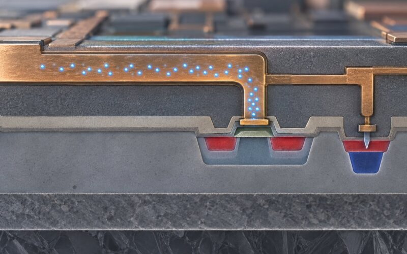
Power reaches a transistor through a chain of connections, each one wider and heavier than the last as you move away from the load. Current converges as it travels toward the cell, and the resistance of each stage adds to the total voltage the cell sees.
The stages, from the outside in, look like this:
| Stage | What it is | What it does |
|---|---|---|
| Package connection | Solder bumps, package balls, wire bonds or flip-chip attaches | Carries current across the package-to-die interface, where the connection count is limited by bump pitch |
| Top-level metal | Thick straps and rings on the upper metal layers | Moves large totals of current with very low resistance and spreads them across the die |
| Middle mesh | A regular lattice of orthogonal wires on mid-level metal | Distributes current regionally, with short paths to any point inside a mesh cell |
| Lower-level rails | Standard-cell VDD and VSS rails on the lowest metal | Feeds each row of cells, at a current density the cell library is designed for |
| Local connection | Via arrays and cell-level power pins | Stitches the layers vertically so current can actually move between them |
The ordering matters more than it looks. Upper metals are thick, so their sheet resistance is low, but they are sparse, so there is a long way to travel. Lower metals are dense, so they reach everywhere, but they are thin, so they resist. A good design uses the wide upper layers to distribute and the dense lower layers to collect.
What Are the Main Power Grid Topologies?
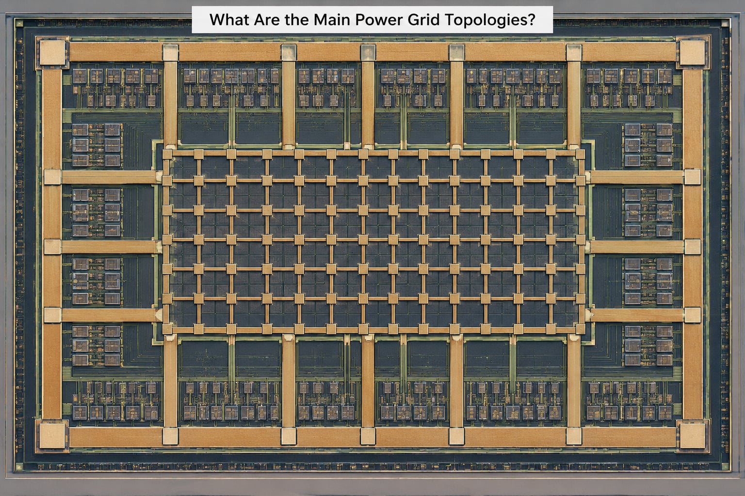
The main power grid topologies are a hierarchical grid, a ring or mesh structure, a hybrid of both, and island-based power domains. None of them is right in isolation; what changes between them is where the wide metal sits and how many parallel paths a load has back to the pads.
Hierarchical grid
Wide straps on the upper metals feed a regular orthogonal mesh on the middle layers, and the mesh feeds standard-cell rails below. The mesh pitch defines the worst-case path length, so tighter pitch means lower local resistance and more routing resource spent on the grid.
Ring structures
A core ring wraps the logic core, and each memory or hard macro gets its own ring around its boundary. Rings are the natural way to feed a macro because they can be sized to the macro’s known current demand, independent of what sits next to it.
Hybrid structures
Most large chips are hybrid: a global strap framework on top, a mesh underneath, and per-macro rings at the leaves. The upper metal carries total current with low loss, the mesh covers everything else, and the rings handle the blocks with the densest demand.
Island and multi-domain structures
Multi-voltage designs split the die into power domains, each with its own rail set, its own ring and its own connection rules. Power gating adds a third rail that switches a domain off entirely, which creates its own inrush problem at switch-on.
Every one of these costs area. Depending on the block and the node, a grid and its straps can take on the order of a fifth to a third of the routable area, and the wide upper metals are taken from the layers that signal nets wanted. That trade is the central tension of the whole discipline.
Why Do Voltage Drop and IR Drop Matter?
IR drop is the voltage lost across a resistance when current flows through it, and the whole law is V = I x R: the bigger the current, the bigger the loss; the bigger the resistance, the bigger the loss.
For a block drawing 200 mA through a path with 20 milliohms of effective resistance, the drop is 0.2 amperes times 0.02 ohms, which is 4 millivolts. Scaled up to a full-chip current of tens of amps through a network resistance of a few milliohms, the same formula produces tens of millivolts of loss, and most of it lands on the cells furthest from the pads.
Here is a worked strap calculation, with the assumptions stated rather than buried. Assume a wide strap on metal 7 with a sheet resistance of 0.005 ohms per square, a length of 500 microns, and a block that needs 1 amp. If the strap is 10 microns wide, the number of squares is 50, so the resistance is 50 x 0.005 = 0.25 ohms. A 0.25 ohm path carrying 1 amp drops 250 millivolts, which is unusable.
Widen the same strap to 100 microns. The number of squares drops to 5, resistance drops to 0.025 ohms, and the drop becomes 25 millivolts. Ten times the width, one tenth the loss, because resistance in a fixed-width-length wire is inversely proportional to width.
Now add vias. A single via contributes a fixed resistance of its own, often tens to hundreds of milliohms, which can dominate the metal. Ten vias in parallel cut that by ten. In practice, going from one via to a 4×4 array across a strap often changes the answer more than any further widening of the metal.
This is the key mental model for power grid design in chips: the answer is never one thick wire, it is many parallel paths with dense vertical connections between them.
Why does losing 30 millivolts matter? Because transistor delay depends on supply voltage. As supply falls, drive current falls, and a cell that met timing at nominal voltage can miss timing at the low end of its allowed range. Noise margin shrinks with it, so a cell that was robust starts producing intermittent wrong answers under temperature and process variation. A design that passes timing at the average supply voltage and fails at the minimum is a design that failed.
How Does Power Grid Design in Chips Explained Apply to Dynamic Power?
Why power grid design in chips must answer di/dt
Dynamic drop is the part of the voltage sag that comes from fast current pulses rather than steady current. Every time a block switches, it draws a burst of current for a fraction of a nanosecond, and the grid’s own inductance resists that change in current. The result is a voltage droop superimposed on the static level.
Average current tells you almost nothing here. A block averaging 200 mA can draw 2 amps for a few hundred picoseconds every cycle, and the second number is what stresses the grid. That is the di/dt problem: a fast current change through parasitic inductance produces a voltage step, and the equation is V = L x di/dt.
| Static IR drop | Dynamic IR drop | |
|---|---|---|
| What causes it | Steady current through resistive metal | Switching current pulses through resistance and inductance |
| Timescale | Steady state, effectively continuous | Picoseconds to nanoseconds |
| Worst case location | Cells furthest from the pads, along the longest resistive path | High-switching blocks, clock networks and memory banks |
| Main effect | Systematic reduction in supply voltage | Transient droop that can push a cell below its functional floor |
| What it hits first | Throughput and timing margin | Timing margin, then functional correctness, then clock distribution itself |
| How it is analysed | DC analysis with a maximum current vector | Vectorless or vector-based transient analysis with switching activity |
The reason static analysis is not enough comes down to where the charge comes from. When a block switches, the current has to arrive immediately. On-chip decoupling can supply a small burst, but only for a short window before the grid itself has to respond. The grid response is bounded by the package inductance, the on-chip capacitance and the bandwidth of the supply regulator, which is why a droop of a few tens of millivolts over a few hundred picoseconds is a normal thing to see in a dynamic power map.
Clock networks are the worst case, because a clock buffer switching is itself a load. Droop in the clock network shows up as skew and jitter on top of the droop in the logic it drives, and a design that looks clean on average power can still fail its jitter budget.
How Do Vias, Wire Width, and Metal Layers Affect the Grid?
Every geometric choice in the grid trades one electrical quantity against another. Widening metal lowers resistance and raises capacitance to neighbouring nets. Moving up a layer lowers resistance and reduces routing density. Adding vias lowers vertical resistance and consumes placement area in the lower layers.
| Change | Electrical effect | What it costs |
|---|---|---|
| Wider wires | Resistance falls roughly in proportion to width; current density drops | More area, more coupling capacitance, less routing room |
| More parallel straps | Effective resistance falls with the number of paths, and no single path carries the full current | Upper metal layers, which are also the best signal routing resources |
| More vias per connection | Via resistance is often the dominant term, so this is the cheapest big win | Routing tracks and cell placement area |
| Moving up a metal layer | Sheet resistance falls, so the same current needs a narrower wire | Fewer tracks per unit area, so usable for distribution rather than local connection |
| Tighter mesh pitch | Shorter worst-case path to every cell, so local resistance falls | The grid becomes a larger fraction of die area |
| More decap area | Lower effective supply impedance, better transient response | Placement area and, on some processes, a manufacturability cost |
One detail catches out beginners: a strap drawn on a single layer without vias to the mesh below it is decorative. Connectivity between layers is what makes the network hierarchical rather than a set of disconnected shelves, and via arrays are where most of the real resistance turns out to live.
What Causes Power Grid Reliability Problems?
Power grid reliability problems are caused by sustained current density, resistive heating, and by voltage itself moving outside the window the circuits tolerate. The first two are lifetime problems that show up after months or years; the third can show up on the first power-up.
Electromigration is the big one. Metal atoms in a conductor are not fixed; a sustained current density above roughly 1 x 10^6 amperes per square centimetre will slowly move them along the direction of flow. Puddles and voids form, the cross-section of the conductor narrows, the current density there rises further, and the result is an open circuit or a short to a neighbour. Lifetime is conventionally expressed through Black’s relationship, in which mean time to failure varies exponentially with current density. Practical signoff asks a narrower question: does the design survive a stated number of years, usually ten, at the worst-case current density?
Joule heating is the quieter companion. Current through a resistor produces heat in proportion to I squared x R, so the hot spot is not where you drew the narrowest wire but where narrow metal carries the most current. That combination feeds electromigration directly, which is why current density and lifetime are always checked together rather than separately.
It helps to separate failure classes, because they are caught by different checks:
- Performance failures: timing closures at the minimum supply voltage, or throughput loss from a reduced drive. Caught by voltage-aware timing analysis.
- Functional failures: intermittent wrong results, corrupted memory writes, resets during switch-on. Caught by dynamic IR drop analysis and in-silicon measurement.
- Lifetime failures: opens and shorts from electromigration. Caught by current density and lifetime checks at signoff.
- Transient failures: overshoot when a domain switches off and inrush when it switches on. Caught by dedicated inrush analysis.
Advanced nodes make all four harder. Thinner metals and lower copper mass raise resistance and current density, lower supply voltage shrinks the legal IR budget, and more domains switching independently multiply the number of transient events to check.
What Role Do Decoupling Capacitors Play?
Decoupling capacitors, usually placed as dedicated decap cells, supply short bursts of current locally so the grid does not have to respond instantly. They are placed near high-switching blocks for that reason: proximity is worth more than total capacitance.
What they really change is the impedance the load sees. A bare resistive grid presents a resistance that grows with distance from the pads. Adding local capacitance turns that into a frequency-dependent impedance that is low over a wide band, so the load no longer depends on the whole network for fast current.
There is a real limit to what on-chip decap can do. On-chip capacitance is small in absolute terms, the routing to it adds resistance, and its response time is short. Past a few hundred picoseconds the charge has to come from off-chip, through the package inductance, which is exactly why dynamic droop shows up in the first few hundred picoseconds after a switching event.
More capacitance is not automatically better. It consumes placement area that would otherwise hold logic, it adds via connections, and its benefit flattens once the local loop resistance dominates. The sizing loop runs the other way: find where the impedance peaks across frequency, add enough capacitance at that point to flatten it, and stop when the area cost stops buying droop improvement.
How Is a Chip Power Grid Designed Step by Step?

A chip power grid is designed in a fixed order that runs from a power budget, through domain partitioning and floorplanning, to an initial mesh, straps and vias, then through post-CTS and post-route analysis to signoff. The order matters because each stage’s assumptions are replaced by better data at the next one.
- Define the power budget. Allocate voltage and power per block before any grid exists, so every block has a number to be checked against later.
- Partition power domains. Assign each block to a domain, decide which domains share a rail, and mark the switching behaviour of each.
- Place the pads and macro rings. Put power and ground bumps where the current will be drawn, and wrap each high-current macro in a ring sized to its demand.
- Build the initial mesh after placement is legal. Set the pitch from the mesh cell size and the area you are willing to spend, then fill it in on the lower and middle layers.
- Add straps and via arrays. Connect the mesh to the upper metal with dense via stitching, and check the vertical resistance, not just the horizontal resistance.
- Place decoupling capacitance. Weight placement toward the blocks with the highest switching activity and the worst distance to the pads.
- Run the post-CTS check. With real buffers and a real clock tree, the switching profile is finally available, and the dynamic picture changes significantly.
- Run post-route analysis. Extracted parasitics, final via arrays, final decaps. This is where violations are localised and fixed.
- Iterate on violations. Widen the local strap, add vias, add decap, or move the macro. Fixing locally is nearly always better than widening globally.
- Sign off with margin. Static IR, dynamic IR, current density and lifetime, inrush, and grid integrity connectivity. Common practice is a design margin of roughly 10% on voltage drop, so the grid has headroom for variation that analysis did not model.
Early analysis is deliberately approximate. Upstream estimates around a power grid cell, run at floorplan stage, are typically accurate to about 20% and are orders of magnitude faster than signoff, so you can compare topology options before committing area. Post-CTS analysis lands near 10% accuracy, and signoff-grade analysis is the only result that should gate tapeout. The usual tooling split runs from commercial power planning inside Innovus and PrimeTime, through dedicated analysis engines such as Voltus, Celsius and RedHawk, to extraction and signoff checks in Calibre xACT. What the numbers mean is worth stating plainly: a green result at floorplan stage is a direction, not a guarantee.
Which Power Grid Metrics Should Engineers Check?
The power grid metrics engineers check are static IR drop, dynamic voltage drop, current density and electromigration lifetime, decap utilisation, inrush, and grid connectivity integrity. Each answers a different question, and a signoff report that shows only one of them has left the others unchecked.
| Metric | Question it answers | What the report should show |
|---|---|---|
| Static IR drop | How low is the supply under maximum DC current? | A drop map with the worst point, the total drop, and margin against the target |
| Dynamic voltage droop | How far does the supply move during a switching burst? | Worst-case droop magnitude and its duration, located on the die |
| Current density | Is any conductor carrying more than it should? | Per-layer maximums with the locations that fail, if any |
| Electromigration lifetime | Will the metal survive the required years? | Worst-case lifetime against the required target, not just a pass or fail |
| Decap utilisation | Is the placed capacitance actually connected and used? | Connected versus total decap, and the impedance curve before and after |
| Inrush | What happens when a domain switches? | Peak inrush current and the voltage response at switch-on and switch-off |
| Grid integrity | Is every rail actually connected to its pad? | Floating rail and missing via reports, which are connectivity bugs, not signal integrity |
A report that gives you a number without a location is not much use. A static IR drop result should be a map you can point at and say fix this cell’s connection, not a single percentage for the whole die.
What Are Common Power Grid Design Mistakes?
The common power grid design mistakes are sizing for average current instead of peak, trusting one global power estimate, placing decaps too far from the loads, using too few upper-layer connections, optimising wire width while ignoring via resistance, and treating a clean average voltage as proof of dynamic integrity.
- Sizing for average rather than peak current. Averages hide the burst that actually moves the voltage. Size against the maximum and the switching profile.
- Trusting a single global power number. A block-level budget with a known distribution is what makes a violation locatable.
- Placing decaps far from the loads. The benefit of capacitance falls off quickly with distance, so placement beats quantity.
- Too few upper-layer connections. Vias between the mesh and the straps are the cheapest large reduction in effective resistance available.
- Ignoring switching density. Blocks with the highest activity cause the deepest dynamic droop even when their average current looks modest.
- Widening metal but checking nothing else. If the via count stays the same, the vias become the bottleneck.
- Over-designing the grid until routing congests. Padding the grid everywhere costs signal routing resources and can make a timing problem out of a power problem.
- Treating a clean average voltage as proof. Average voltage tells you nothing about a millivolt-scale transient; that requires dynamic analysis.
A design can pass DRC, pass LVS, and pass a static power check, and still fail because of dynamic droop or because a rail was left floating somewhere. Those are different classes of bug and they need different checks.
Frequently Asked Questions
Why are power and ground both routed as grids in chips?
Because current needs an outgoing and a return path, and every volt dropped on the way out is a volt dropped on the way back. Building both the supply and the return as wide, low-resistance networks keeps the loop area small, which limits parasitic inductance and therefore the transient voltage step during switching. A tight return path also keeps return current close to the signal it serves, which cuts coupling into adjacent nets. A single supply rail with an improvised return will not behave the same way.
Is a wider power wire always better for reducing IR drop?
No, because resistance is only one term in the path. A wide strap on one layer with a single via to the mesh below it can still be dominated by that via’s resistance, which is often tens to hundreds of milliohms against a strap in the milliohm range. Widening also costs area, adds coupling capacitance to neighbours, and steals routing resources. Widening, via arrays, and a proper layer mix all have to be checked together, because a fix that helps one stage can leave the bottleneck somewhere else.
What is the main difference between static and dynamic IR drop?
Static IR drop comes from steady current flowing through resistive metal, so it is a continuous reduction in supply voltage that is worst at the cells furthest from the power pads. Dynamic IR drop comes from fast switching current pulses and from the inductance of the path, so it is a short transient droop that is worst at high-switching blocks, clock networks and memory. Static is found with a DC analysis and a maximum current vector; dynamic needs transient analysis with real or estimated switching activity. A design can pass one and fail the other.
How many power grid layers does a modern chip need?
There is no fixed number, and the honest answer depends on the current budget, the voltage budget and how much area you are willing to spend. What matters is a hierarchy: dense lower metals for local connection, a mid-level mesh sized so the worst-case path stays short, and thick upper metals for moving total current off the die. Small analog and IO blocks may work with two or three usable layers, using wide rails and rings instead of a mesh. Large designs typically use the full metal stack in a layered structure.
Can software-only fixes resolve power grid voltage-drop violations?
Not the underlying network, and this is a common source of wasted effort. Compiler directives, voltage-aware optimisation and clock gating can reduce the current that causes the drop, and they are worth trying first because they cost no area. But if the network resistance itself is too high, no amount of scheduling fixes it; the metal has to get wider, the via count higher, or the decap closer. A good workflow tries the zero-area fixes first, then spends area on the physical grid where the drop map says it is needed.
How do power grid results change at advanced process nodes?
Everything gets harder in the same direction. Thinner metals mean higher resistance and higher current density for the same current, lower supply voltage shrinks the legal IR budget, and more independent power domains create more transient events to check. The compensation is that more metal layers are available and the upper layers are proportionally better conductors, so the answer is more aggressive use of the upper stack plus denser via stitching, paid for with area. Current density and lifetime checks also tighten, since thinner metal has less mass to move.
Conclusion
The mental model to keep is that a chip power grid is a resistance-management problem solved by redundancy and layering, not one thick wire. Wide upper metal moves the total current, a mid-level mesh spreads it, dense vias join the layers, and local decaps handle the fast part.
If you are starting a new block, do four things in this order. Build a current profile rather than a single number, including the switching behaviour. Set a voltage budget and a design margin before drawing metal. Choose a hierarchical topology and the layers it needs, and check what that costs in routable area. Then iterate on extracted static and dynamic analysis, fixing violations locally where the map points rather than by widening the whole grid.
Academic treatments worth working through for the formal version of this material include the IRAJ review of power grid analysis in integrated circuits, F.N. Najm’s ISPD slides on physical design challenges in the chip power distribution network, and the Nassif power grid analysis benchmarks.