A linear regulator burns the excess input voltage as heat to hold its output steady, while a switching regulator chops the input with a high-frequency transistor and rebuilds it through an inductor, moving nearly all the input energy to the load instead of the heatsink. Those switching vs linear regulator differences decide almost every power tree decision: how much of your battery budget you waste, how much copper area you need for heat, and whether your analog signals pick up switching ripple. Here is the practical version of the comparison, with numbers instead of adjectives.
Table of Contents
- Switching vs Linear Regulator Differences at a Glance
- Efficiency and Power Conversion Loss
- How Switching and Linear Regulators Handle Losses
- Where switching vs linear regulator differences get smaller
- Output Noise and Ripple
- Transient Response and Load Regulation
- Circuit Complexity and Board Design
- Thermal Performance and Current Capacity
- Which Should You Choose?
- Frequently Asked Questions
- What are the key differences between linear and switching regulators?
- How do I know if my power supply is linear or switching?
- What are the disadvantages of a linear regulator?
- When should I use an LDO instead of a switching regulator?
- Can a linear regulator be placed after a switching regulator?
- Why does my supposedly quiet LDO oscillate or ring?
- Conclusion
Switching vs Linear Regulator Differences at a Glance
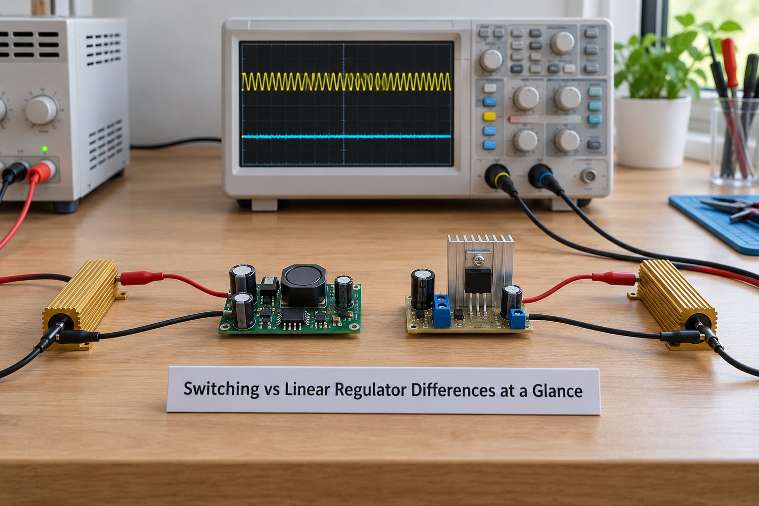
Short version: switching wins on efficiency and current capability, linear wins on output noise and simplicity, and a switching stage feeding a low-dropout regulator often beats both.
| Criterion | Linear regulator | Switching regulator |
|---|---|---|
| Conversion efficiency | Approximately Vout divided by Vin, so 5 V to 3.3 V is about 66% | Typically 80% to 95% across the useful load range |
| Output noise and ripple | Microvolt to millivolt level, broadband but very low | Millivolt ripple at the switching frequency plus wideband noise |
| EMI | Minimal conducted or radiated emissions | Requires layout discipline, filtering and often shielding |
| Direction | Step-down only | Step-down (buck), step-up (boost) or both (buck-boost) |
| Input-to-output range | Output must sit below input by at least the dropout voltage | Wide ranges, often 5.5 V down to sub-1 V in one part |
| Load transient response | Fast, simple loop, no phase margin surprises | Fast when designed for it, but depends on loop compensation |
| Quiescent current | Tens to hundreds of microamps typical | Tens of microamps in power-save mode, more in continuous operation |
| Component count | Input and output capacitors, feedback divider if adjustable | Adds an inductor, a Schottky or synchronous FETs, and compensation |
| PCB area | Small, but a large copper pour or heatsink may be needed | Larger footprint, tight layout for the switching loop |
| Thermal behaviour | Heat scales with the dropped voltage times load current | Losses are small and mostly in the switches and inductor |
| Design effort | Hours | Days, especially layout and compensation |
| Best suited to | Low-noise analog rails, RF bias, sensor and reference supplies | Processor rails, battery devices, high current, any large voltage step |
One row deserves a warning label. Linear regulation of a 5 V rail down to 3.3 V throws away roughly a third of the input power as heat, and no layout trick recovers it. That single number decides most designs.
Efficiency and Power Conversion Loss
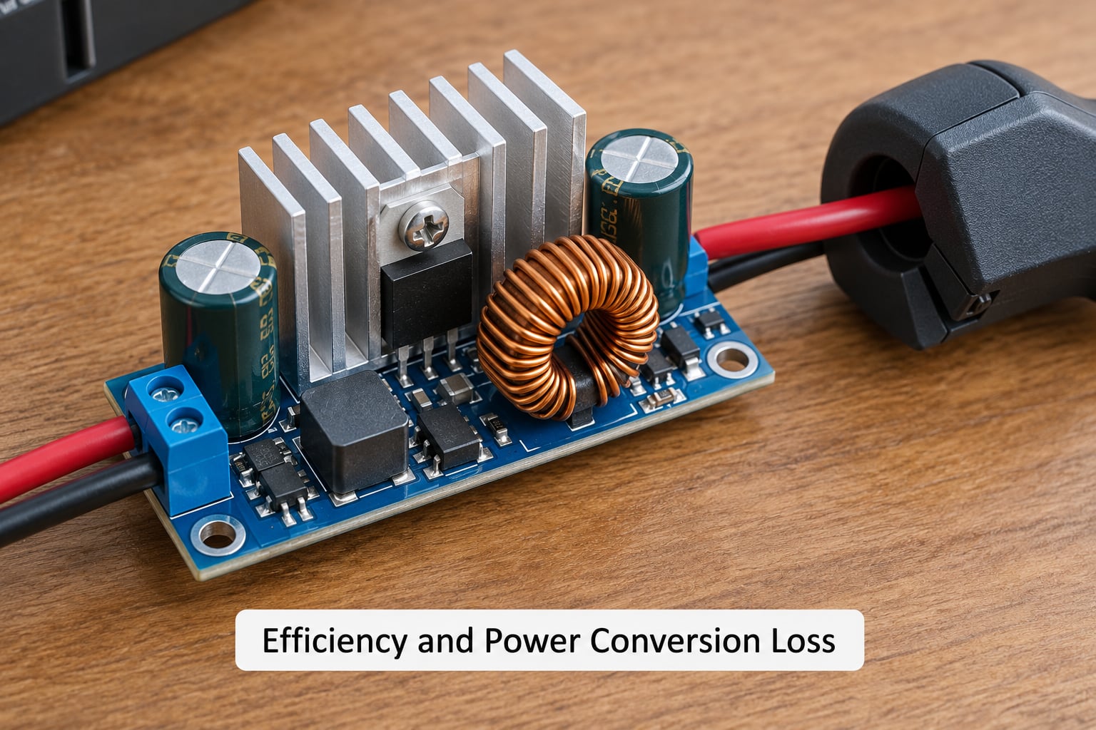
A linear regulator cannot do better than Vout divided by Vin, because the difference between the two voltages is dropped across a pass transistor and turned into heat. The heat number follows directly: power dissipated is the input-to-output voltage difference times the load current.
Worked example, 5 V in, 3.3 V out at 300 mA. Efficiency is 3.3 divided by 5, so 66%. Dissipated power is 1.7 V times 0.3 A, which is 0.51 W from a supply that is only 1.65 W to begin with. That is a small hot spot on a board that has room, and a serious problem in a sealed enclosure.
The ratio matters more than the load. At 3.3 V out from 5 V in you lose about a third. At 1.8 V out from 5 V in the same linear part delivers 36% efficiency and dumps 0.96 W for every watt you use. A phone or a sensor node running a 4.2 V cell down to 1.8 V is deep in the worst case for a pure linear solution.
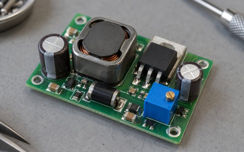
Switching converters move energy inductively rather than resistively, so their losses come from switch on-resistance, gate charge, inductor resistance, and capacitor ESR. That is why 85% to 92% is routine, and why a switching converter beats a linear one by a wide margin whenever the voltage step is large. The gap closes as the step shrinks, which is worth understanding before you default to one or the other.
How Switching and Linear Regulators Handle Losses
Four loss mechanisms matter, and they behave differently.
Conduction loss dominates in linear regulators and scales linearly with current. Halve the load current and you halve the heat. In switching regulators the equivalent is the on-resistance of the high-side and low-side FETs, which is why the efficiency curve is flat across most of the load range.
Switching loss scales with frequency and transition time. Every cycle the FETs cross the voltage across them while dissipating power, so losses rise with switching frequency. That is the tradeoff a switching designer makes deliberately when choosing a 2 MHz part over a 500 kHz part.
Quiescent current is the current the regulator draws from the input when the load is near zero. For a battery device this sets the floor on standby life. A 40 microamp part drawing from a 220 mAh coin cell removes roughly 1 mAh a day, which is under half a percent of the cell spent doing nothing. Low-Iq parts exist on both sides of this comparison, but the linear architecture reaches lower numbers more easily because there is no oscillator to keep running.
Dropout voltage is the headroom the pass transistor needs before it can control. A conventional linear regulator might need 1 V or more, which rules it out for low-headroom conversion. A low-dropout regulator is a linear regulator designed for a dropout of a few tens of millivolts, which is what makes the hybrid architecture below possible.
Where switching vs linear regulator differences get smaller
Two cases narrow the gap, and both show up constantly in real designs.
Small voltage steps. Regulating 5 V down to 4.5 V with a linear part gives about 90% efficiency and only 150 mW of heat at 300 mA. That is often simpler and quieter than adding a switching stage and its inductor, so a linear part is a legitimate choice even when efficiency is nominally on the table.
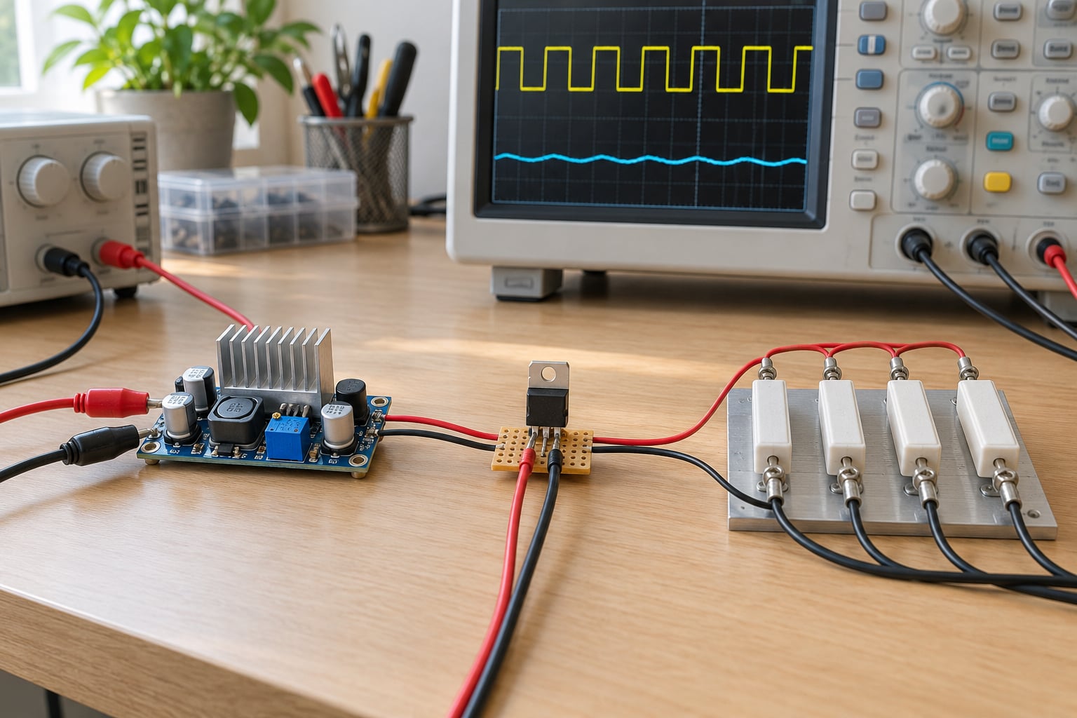
The hybrid chain. Feed a low-dropout regulator from an efficient switching pre-regulator that drops the input to within a few hundred millivolts of the target. The switching stage does the big voltage reduction at high efficiency, the LDO burns only its dropout, and the final output is clean. This is the standard answer for quiet-and-efficient rails, and it is why you will see a two-stage power tree in RF and audio designs. The cost is two active parts, a larger footprint, and one more failure mode to check.
Output Noise and Ripple
Linear regulators are quieter because nothing is switching. What reaches the output is reference noise, pass-device noise, and the input supply’s own disturbance attenuated by the loop. Output noise in the tens of microvolts RMS is normal for a good low-noise LDO at low dropout, and it is broadband rather than concentrated at one frequency.
A buck converter puts deliberate ripple on its output. The inductor smooths the current, and the output capacitor plus the loop shape the voltage, but some ripple always remains at the switching frequency. A well-designed converter with 20 to 40 microfarms of ceramic and ceramic input filtering can get to a few millivolts peak-to-peak, roughly two orders of magnitude worse than an LDO on the same rail. Alongside that sits wideband switching noise that couples readily into sensitive analog through shared ground impedance.
The honest complication, and one that comes up repeatedly in engineer forums: the difference is not purely architectural. Plenty of supposed low-noise LDOs ring or oscillate into capacitive loads because of output capacitance limits and stability issues, and plenty of switching rails pass their own noise specs until you route the feedback trace next to the inductor. Layout mistakes get blamed on the regulator type constantly. Before you conclude an LDO is too noisy, check that the output capacitor falls inside the stability window in the datasheet and that the feedback trace is short and quiet.
The way to fight buck noise on an analog rail is to switch at a frequency well above your signal bandwidth and filter it down. If your ADC reference matters up to 1 kHz and the converter runs at 1 MHz, a simple LC filter on the output removes most of the ripple and leaves the noise floor of the regulator itself. That works, but it costs board area, and the filtering is less forgiving than simply using a clean source.
Transient Response and Load Regulation
Load regulation is how well the output holds its voltage when current changes. Both architectures can do it well; they get there by different mechanisms.
A linear regulator loop is slow in one sense and fast in another. There is no inductor and no output charge to recover, so the pass transistor simply conducts more current. The response is limited by how fast the error amplifier and pass device can react, which is usually enough for analog loads. There is a hidden risk: driving too much output capacitance can destabilize the loop entirely, which is the ring engineers complain about.
A switching converter must charge the output capacitor through the inductor during a load step, and inductance resists a sudden change in current. Its loop bandwidth is set by the compensation network the designer chooses, and vendor parts are often optimized for steady-state ripple rather than for a hard 10 A step. Faster response usually means crossing the loop closer to the switching frequency, which costs phase margin and raises output ripple. That is the real tradeoff in transient response: you cannot buy both fast settling and low ripple from the same loop without paying for it elsewhere.
Load regulation itself is comparable once the feedback divider is designed well. Both types drift as temperature changes, both can be trimmed, and both put the divider’s input current directly into the output error budget. Keep divider currents in the microamp range if your rail needs microvolt accuracy.
Circuit Complexity and Board Design
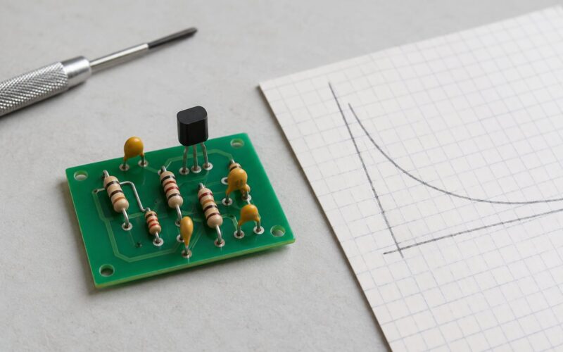
A linear regulator is two capacitors and possibly a divider. You choose its package, route the input and output, and check the copper area against the dissipation. There is no switching node, no layout constraint that will bite you at 2 am, and no filter to tune.
A switching regulator adds an inductor, its current rating has to match the peak load rather than the average load, and the input capacitor must sit within a few millimeters of the high-side FET. The hot loop between input capacitor, high-side FET, low-side FET and ground has to be as small as the layout rules allow, because its parasitic inductance is what generates the voltage spikes that show up on your oscilloscope. Place the inductor away from the feedback divider, and keep the analog ground reference at the quiet end of the layout rather than at the converter’s ground return.
EMI filtering is a second order of work. Switching nodes radiate, and conducted noise travels back up the input rail into whatever else is fed from it. Filtering helps but never fully compensates for a poor hot loop, which is the opposite of how layout advice is usually phrased. Plan for a filter footprint even if you populate it with a shorting link at first.
Component count drives board area and cost more than the regulator price does. A switching design needs roughly three to five times the passives of a linear one, and the inductor is usually the most expensive item on the bill. For a tight wearable or a coin-cell node, that footprint difference can decide the architecture on its own.
Thermal Performance and Current Capacity
Linear regulators have a hard thermal ceiling that follows directly from the physics. The pass transistor dissipates the dropped voltage times the load current, and the part has a maximum junction temperature and a maximum allowable dissipation set by its package and its thermal resistance to the board. When dissipation exceeds that, current capability drops.
A concrete case: a 3.3 V to 1.8 V linear regulator rated for 500 mA cannot actually deliver 500 mA in a small package. At 1.5 V of dropout and 500 mA you would be asking for 0.75 W, which needs a substantial copper pour or an external heat spreader. Designers routinely derate these parts by half or more once thermal limits are included, and that derating is where linear solutions quietly fail. A thermal shutdown or a foldback current limit protecting an overloaded part is a system design telling you the topology was wrong.
Switching converters move the same current with far less heat, so their current capability is limited by the inductor, the FETs and the layout rather than by a big voltage drop. A 10 A converter running from 5 V to 3.3 V dissipates on the order of a watt in total, spread across two switches and an inductor, instead of 17 W in one pass transistor. That is why a 10 A load essentially forces a switching solution, and why thermal design so often decides the architecture before the datasheet numbers do.
Switching designs still need thermal care. Inductors have saturation and temperature-rise limits, and the high-side FET sees the full input voltage during every transition. Give both parts airflow and copper, and check the ambient inside the enclosure rather than outside it.
Which Should You Choose?
Match the architecture to the rail’s job, then check the numbers on the datasheet against the list below.
Low-noise analog rails: use a linear regulator, or an LDO after a switching pre-regulator. Reference voltages, ADC and DAC supplies, and microphone or sensor bias rails fall here. The switching fallback is acceptable when the converter runs far above your signal bandwidth and you can afford the output filter.
RF front ends and oscillators: use a linear regulator with a high power supply rejection ratio at your operating frequency. LDO PSRR usually rolls off well above the kilohertz range, and a noisy bias rail will show up as phase noise or as spur lines in a spectrum analyser. Check the PSRR curve against the band you care about, not the headline number.
Battery-powered devices: the primary constraint is the product of quiescent current and standby hours. Compare both architectures at your real light-load current, not at the headline mid-load efficiency, because power-save and pulse-skipping modes change the picture completely below roughly 10% of full load. When the current is genuinely tiny and steady, a switched-capacitor charge pump is often the better third option: high efficiency at light load, no inductor, but limited current and more output ripple than a regulator.
FPGA, processor and accelerator rails: use a switching converter, almost always. The currents are large, the voltage steps are wide, and multiple rails need sequencing with soft-start and power-good. Follow the vendor’s recommended regulator footprint and decoupling exactly, because stability and current sharing depend on the specified layout.
Compact portable systems: choose on area. If the linear solution fits and the dissipation fits its copper, take the quieter, simpler one. If it needs a heatsink, take the switching part and spend the saved area on filtering instead.
Thermal-limited enclosures: switching, without exception. If the enclosure has no path to shed watts, the linear design’s losses become the system’s limiting factor.
Frequently Asked Questions
What are the key differences between linear and switching regulators?
A linear regulator passes the input through a pass transistor and burns the difference between input and output voltage as heat, so its efficiency tops out near Vout divided by Vin and it can only step voltage down. A switching regulator uses a high-frequency transistor and an inductor to move energy, reaching roughly 80% to 95% efficiency and supporting step-up, step-down or both, at the cost of output ripple, EMI and a more demanding layout.
How do I know if my power supply is linear or switching?
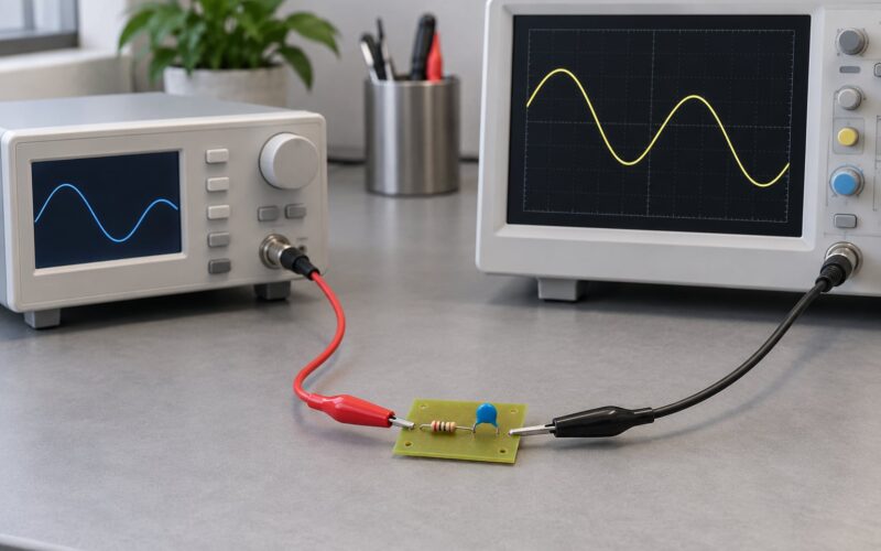
Listen first: a switching regulator produces audible or high-frequency acoustic noise around its switching frequency, while a linear supply is silent. On the scope, look at the output with a probe shorted to ground. A linear rail shows only slow drift; a switching rail shows periodic ripple at the switching frequency. You can also feel for heat: a linear regulator dissipates the dropped voltage times the load current, so it runs noticeably warm under load.
What are the disadvantages of a linear regulator?
Efficiency falls as the voltage step grows, since dissipation equals the input-to-output voltage difference times load current. That heat limits current capability and forces copper area or a heatsink. A linear regulator also cannot step voltage up at all, and its dropout voltage sets a hard limit on how little headroom it needs to work.
When should I use an LDO instead of a switching regulator?
Use a low-dropout regulator when the rail is noise-sensitive, the voltage step is small, and the load current is modest. Typical cases are RF and sensor bias, analog references, audio and precision instrumenting. If the step is large or the current is high, the LDO will overheat, so use a switching converter or a switching pre-regulator feeding an LDO post-regulator.
Can a linear regulator be placed after a switching regulator?
Yes, and it is the standard hybrid architecture. The switching converter first reduces the input to within a few hundred millivolts of the target, so the LDO only drops its own dropout voltage and stays cool. The output is then nearly ripple-free, giving clean, efficient power in one chain at the cost of two active parts and a larger board area.
Why does my supposedly quiet LDO oscillate or ring?
Almost always the output capacitor is outside the stability window the datasheet specifies, often because a designer substituted a lower capacitance or lower ESR part. Check the permitted output capacitance range, keep the feedback divider currents low, and confirm the regulator has enough phase margin for the load. If it is stable on the bench and rings in the product, suspect ground impedance or a long feedback trace.
Conclusion
Work through the constraints in order rather than picking a favourite architecture. Start with the conversion ratio, because a large step makes a linear stage expensive in heat before anything else matters. Then check the noise limit of the load against ripple and PSRR at the frequency you actually care about, define the load behaviour so you can judge transient response, and set the thermal budget against your enclosure. Finally, check the board constraints, since passives, layout rules and EMI filtering all cost area.
Most designs land cleanly once those five are written down. Quiet analog rail with a small step, linear or LDO. Large step or large current, switching. Both requirements at once, a switching pre-regulator into an LDO, with the datasheet numbers checked against your own light-load and worst-case conditions rather than the headline figures.