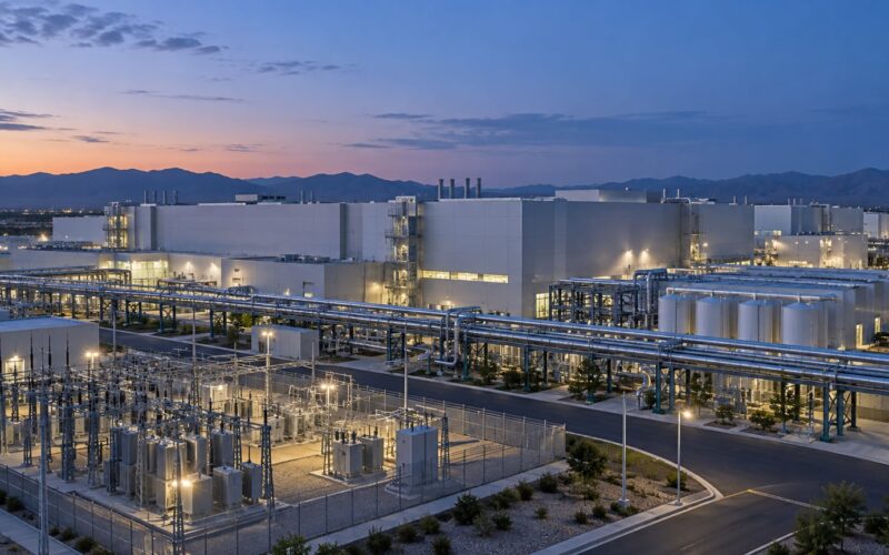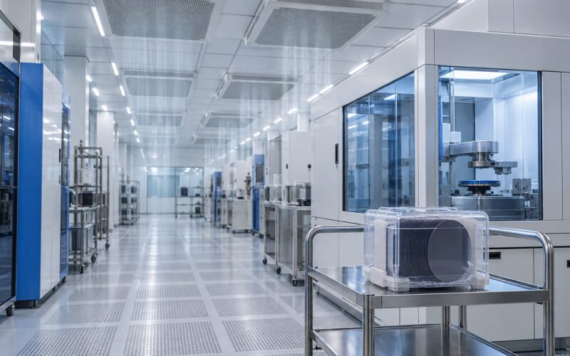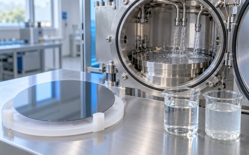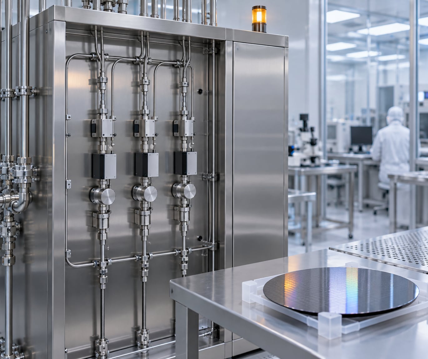
What gases are used in chip manufacturing? Chip fabs run on ultra-high-purity process gases grouped into five functional families: deposition, etching, dopant, chamber cleaning, and inert or carrier. Nitrogen is the one gas every fab consumes by the tonne, and everything from silane to sulfur hexafluoride is chosen for a specific chemistry step on the wafer.
Below is a working reference: what each gas does, which fabrication step consumes it, and why purity and delivery decide whether a wafer comes off the tool good or scrapped.
Table of Contents
- What Gases Are Used in Chip Manufacturing?
- Common Gases Used in Wafer Fabrication
- Gases for Etching and Patterning
- Fluorine chemistry for silicon and dielectrics
- Chlorine and bromine chemistry for conductors
- Why etchants are the gases that need abatement
- Gases for Thin-Film Deposition
- Silicon-bearing gases
- Nitrogen and halogen chemistry for dielectrics
- Inert carrier gases in deposition
- Gases for Cleaning, Annealing, and Photoresist Processing
- Chamber and wafer cleaning
- Annealing and thermal steps
- Lithography and drying
- Why Gases Are Used Instead of Liquids or Solids
- How Gas Purity and Delivery Affect Chip Yield
- What ultra-high purity actually means
- Moisture, oxygen and particles
- How gases reach the chamber
- Safety and Environmental Considerations
- Pyrophoric and toxic gases
- Environmental impact of fluorinated gases
- Supply concentration
- Frequently Asked Questions
- Which gas is used most in chip manufacturing?
- Is nitrogen used in silicon chip fabrication?
- Which gas is known as the killer gas?
- Why are noble gases important for chipmaking?
- How do process gases differ from liquid chemicals in a fab?
- Do all chips use the same gases?
- What to Take Away
What Gases Are Used in Chip Manufacturing?
Three kinds of gas move through a wafer fab. Process gases react, etch or deposit material. Carrier gases move and dilute those reactants without joining them. Purge gases flush lines and chambers between steps.
Nitrogen (N2) sits across all three roles. It purges gas lines, blankets wafers between lithography steps, dilutes reactive mixtures, and acts as a carrier gas during deposition. Hydrogen (H2) and oxygen (O2) are used more narrowly: hydrogen for annealing and as a reducing agent, oxygen for descumming and photoresist stripping.
The exact mix is never fixed. It changes with the process flow, the tool manufacturer, the material layer being built, and the target node. A mature 28 nm logic flow and a 2 nm logic flow use overlapping gases, but the newer node leans harder on halogenated etch gases and on deposition chemistries that carry their own oxidant or reducing agent.
Common Gases Used in Wafer Fabrication
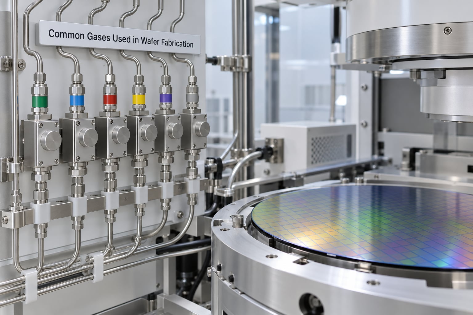
This table maps the main gases used in chip manufacturing to their role and the step that consumes them. Formulas are given alongside names because that is how process engineers write them.
| Gas | Formula | Role | Where it is used |
|---|---|---|---|
| Nitrogen | N2 | Carrier / purge | Line purge, chamber purge, lithography blanketing, deposition carrier |
| Hydrogen | H2 | Process / carrier | Annealing, epitaxy ambient, reducing agent, resist stripping |
| Helium | He | Carrier / cooling | Carrier gas in deposition, wafer cooling and heat transfer |
| Argon | Ar | Process / carrier | Sputter target gas, physical ion etch, chamber conditioning |
| Oxygen | O2 | Process | Descumming, photoresist ashing, oxide growth |
| Ozone | O3 | Process | Oxidation in diffusion furnaces, surface cleaning |
| Ammonia | NH3 | Process | Silicon nitride and silicon oxynitride deposition |
| Silane | SiH4 | Process | Silicon deposition, poly gates, spacers, epitaxy |
| Trichlorosilane | HSiCl3 | Process | Epitaxial silicon, source and drain deposition |
| Nitrous oxide | N2O | Process | Oxynitride deposition, resist hardening |
| Diborane | B2H6 | Process | Doping, boron silicide formation |
| Phosphine | PH3 | Process | N-type doping, poly gate doping |
| Arsine | AsH3 | Process | N-type dopant, silicon carbide nucleation |
| Sulfur hexafluoride | SF6 | Process | Selective etching of silicon and silicon dioxide |
| Carbon tetrafluoride | CF4 | Process | Silicon dioxide and nitride etching |
| Trifluoromethane | CHF3 | Process | Dielectric etching, contact hole cleaning |
| Octafluorocyclobutane | C4F8 | Process | Highly selective dielectric etching |
| Nitrogen trifluoride | NF3 | Process | Chamber cleaning, remote plasma clean |
| Chlorine | Cl2 | Process | Metal and conductor etching |
| Hydrogen bromide | HBr | Process | Silicon etching, single-crystal source and drain |
| Boron trichloride | BCl3 | Process | Metal gate etching, boron doping |
| Neon | Ne | Carrier | Excimer laser gas mix for lithography |
| Krypton and xenon | Kr, Xe | Carrier | Excimer laser gas mixes for lithography |
Two things stand out. Nitrogen is everywhere because it is cheap, inert and easy to purify to absurd levels. Everything else is present for one reason only: its chemistry.
Gases for Etching and Patterning
Etching is where gas choice becomes chemistry rather than logistics. The gas family you pick decides what you remove, what you leave alone, and whether the sidewall is vertical or re-deposited.
Fluorine chemistry for silicon and dielectrics
Fluorine atoms are aggressive toward silicon and silicon-based dielectrics. Sulfur hexafluoride (SF6) carves silicon trenches and opens oxide, and it etches silicon preferentially to silicon dioxide, which is exactly what a contact or via cut wants. Carbon tetrafluoride (CF4) is the generalist dielectric etchant for silicon dioxide and nitride.
Selectivity is the trade. CF4 etches oxide fast but not selectively enough on its own, so trifluoromethane (CHF3) is added to polymerise a protective fluorocarbon film on the sidewall. More CHF3 means a more vertical profile and slower removal. Octafluorocyclobutane (C4F8) pushes that further, giving very high selectivity for cutting deep, narrow features without collapsing the pattern.
Chlorine and bromine chemistry for conductors
When the target is a metal rather than an oxide, the halogen switches. Chlorine (Cl2) etches aluminium and tungsten smoothly. Hydrogen bromide (HBr) is the standard etchant for crystalline silicon, used for isolated source and drain structures where ion damage has to be kept low. Boron trichloride (BCl3) etches metal gates and supplies boron for in-situ doping, because it also deposits boron as it reacts.
Adding oxygen to a halogen mixture is common. It changes the polymer chemistry on the sidewall and gives engineers another handle on selectivity.
Why etchants are the gases that need abatement
Perfluorocompounds such as CF4, C4F8 and CHF3 are stable in the atmosphere. When they leave an exhaust line, they act as greenhouse gases rather than breaking down, which is why fabs plumb etch tool exhaust into abatement systems rather than venting it.
Gases for Thin-Film Deposition
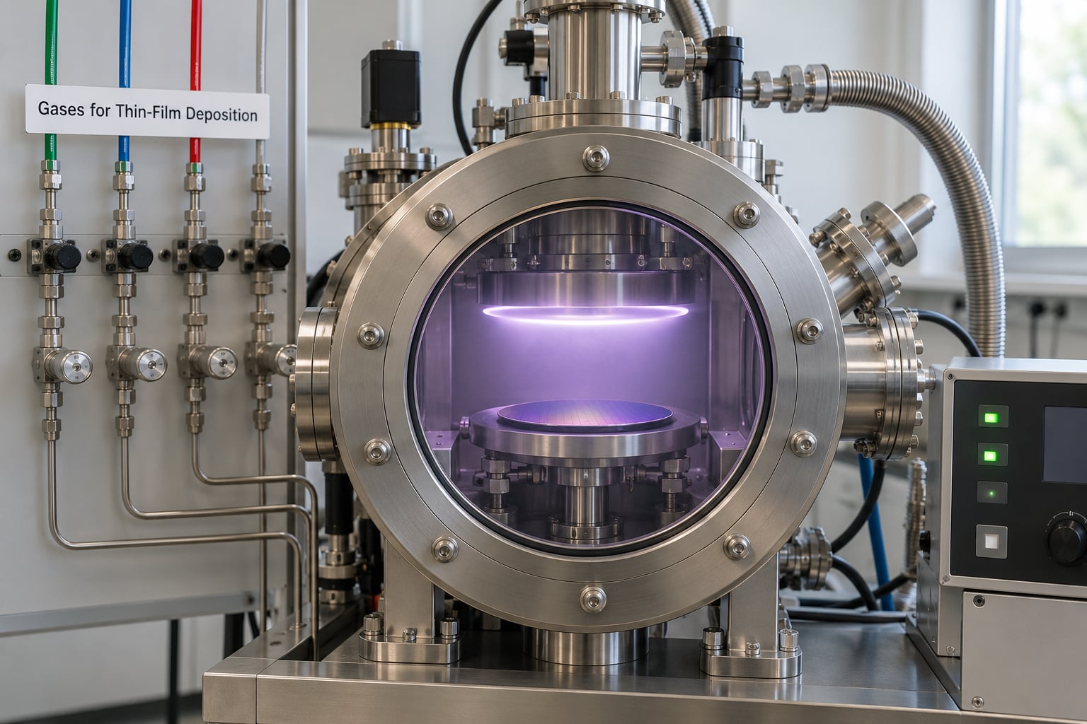
Deposition gases are the ones that stay on the wafer. That makes them the hardest purity problem in the fab, because every impurity the gas carries becomes a defect in the film.
Silicon-bearing gases
Silane (SiH4) is the workhorse. Plasma-enhanced chemical vapour deposition runs silane with nitrous oxide to lay down silicon dioxide and silicon oxynitride, and with nitrogen or argon to lay down doped polysilicon gates and spacers. Trichlorosilane (HSiCl3) carries higher deposition rates, so it dominates epitaxial growth and the source and drain steps where a wafer needs hundreds of nanometres of silicon quickly.
Nitrogen and halogen chemistry for dielectrics
Ammonia (NH3) reacts with silane to form silicon nitride, either as a hard etch-stop layer, as the liner in a modern interconnect stack, or as the final passivation over a finished device. Chlorosilanes such as trichlorosilane and dichlorosilane carry different silicon-to-chlorine ratios, which changes film stoichiometry, stress and chlorine content.
Inert carrier gases in deposition
Argon (Ar) sputters metal targets for aluminium, copper and tantalum. Helium (He) and nitrogen (N2) carry the reactive species in deposition and conduct heat away from the wafer. In atomic layer deposition, a high-purity nitrogen carrier separates the precursor pulses, and hydrogen (H2) can act as a reducing purge to strip ligands from the surface between cycles.
Gases for Cleaning, Annealing, and Photoresist Processing
Not every gas builds something. A large share of fab gas consumption goes into removing residue, repairing damage and holding surfaces in a known state.
Chamber and wafer cleaning
Oxygen-based chemistry removes organic film. Photoresist that has been exposed and developed away leaves a thin polymer layer on the wafer, and it is stripped in an oxygen plasma or an ozone treatment. Inside the tool, nitrogen trifluoride (NF3) is the preferred chamber clean because it reacts with silicon nitride and oxide residues without the heavy fluorocarbon polymer by-products that CF4-based cleans leave behind.
Annealing and thermal steps
Hydrogen (H2) anneals damage out of silicon and passivates dangling bonds at the silicon-to-dielectric interface. Nitrogen (N2) provides the inert ambient for furnace steps and rapid thermal processing, and it protects surfaces during cool-down.
Lithography and drying
Nitrogen blanket gas flows over the wafer during exposure steps to control temperature and prevent contamination between the track and the scanner. Helium (He) has a role in heat transfer and in some advanced thermal regimes, and nitrogen is the standard drying medium after wet cleans because it displaces water without leaving ionic residue.
Why Gases Are Used Instead of Liquids or Solids
Every chemistry here could in principle be run as a liquid bath or a solid source. Gases win for six practical reasons.
- Metered delivery. A mass flow controller meters gas flow in standard cubic centimetres per minute and can swing from a few hundred sccm to a milli-sccm during a step. Liquids do not meter that precisely across a wafer.
- Vacuum compatibility. Etch and deposition chambers run at fractions of a torr. A gas goes straight in; a liquid would flash across the wafer and contaminate it.
- Fast switching. Valve open, valve closed. Recipe steps change in under a second, which is what makes atomic layer deposition possible.
- Reactive plasma generation. RF energy ionises the gas in place. You cannot make a plasma out of a bath.
- Purity. Distillation and adsorption techniques take a bulk gas to parts-per-billion impurity levels and hold it there.
- Uniform flow across a wafer. Showerhead gas distribution gives a predictable composition at every point on a 300 mm surface.
The trade-off is safety. Handling a gas means managing a compressed or liquefied container of something that can poison, corrode or ignite.
How Gas Purity and Delivery Affect Chip Yield
A defect is expensive. A single particle can kill a wafer carrying days of process work, so gas purity is treated as a process parameter, not a purchasing detail.
What ultra-high purity actually means
Ultra-high purity, or UHP, means impurity levels in the parts-per-billion range for the most sensitive gases, with nitrogen and helium often specified to parts per trillion. Every stage of delivery matters: the bulk supply, the distribution system, the gas cabinet at the tool, and the purifier at the point of use.
Moisture, oxygen and particles
Water and oxygen are the usual contaminants, and both cause traceable failures. Moisture hydrolyzes silane and chlorosilanes into particulate that falls onto the wafer. Trace oxygen perturbs the stoichiometry of an oxide film. Particulates come from the gas itself, from the delivery line, or from the tool, so lines are electropolished stainless steel with validated cleanliness rather than simply clean.
How gases reach the chamber
Bulk gases are produced at very high volume and usually generated on site. Commentary in the Hacker News thread on the TSMC Arizona outage noted that fabs run on-site nitrogen, oxygen and argon from a custom-built air separation installation, because trucking liquid nitrogen across a site is slower and less controllable than making it next door. Helium is the exception, since it comes from geological sources and is delivered as a cryogenic liquid.
Specialty gases are different. Silane, arsine, phosphine and the halogen mixtures are made in small quantities, purified to a harder specification, and delivered in cylinders or in bulk trailers to a gas cabinet. Point-of-use purification adds a final gettering or adsorption step right before the chamber for the gases where parts-per-billion matters most.
Knowing the difference matters more than it sounds. Bulk gases are a facilities and cost problem, measured in tonnes and predictable. Specialty gases are a process-engineering problem, measured in parts-per-billion purity and choice of the right molecule for the layer.
Safety and Environmental Considerations
Some of these gases would be a serious hazard anywhere, and a fab concentrates them in one building.
Pyrophoric and toxic gases
Silane, phosphine, arsine and diborane ignite on contact with air at low concentrations. Arsine is acutely toxic, which is why its industry nickname is the killer gas. Phosphine is used as a fumigant elsewhere in the world, which says a lot about what it does to people at concentration. These gases sit in gas cabinets with automatic shutoff valves, dedicated exhaust scrubbers, and monitors that trigger facility-wide alarms on detection.
Chlorine and hydrogen bromide are corrosive and toxic in their own way. Every toxic or flammable gas is delivered through a cabinet with continuous monitoring, automatic cylinder changeover and a dedicated exhaust path that never shares with room air.
Environmental impact of fluorinated gases
Fluorinated process gases are a real emissions problem. Their global warming potentials are far above carbon dioxide: reported figures put NF3 around 16,000 and SF6 above 23,000 on a 100-year basis, against 1 for carbon dioxide. Because a single etch step can consume tens of kilograms of these gases, regulators count them directly as Scope 1 emissions.
The industry response is abatement. Point-of-use thermal or chemical treatment destroys most of the fluorinated exhaust at the tool, and global warming potential reduction rules allow some credit for it. Substituting lower-GWP molecules where the process allows it is the other lever, which is part of why octafluorocyclobutane chemistry has grown despite being one of the more expensive etchants.
Supply concentration
Neon, krypton and xenon go into excimer laser gas mixes for lithography, and their supply is geographically concentrated. Reporting has put a majority share of semiconductor-grade neon production in Ukraine at various points, with meaningful shares of krypton and xenon from the same region. The 2022 invasion of Ukraine made the concentration briefly visible to consumers, since neon is what gives fluorescent lamps their glow.
Substituting a noble gas is not simple. They are chemically inert, so in principle the recovered gas could be recirculated, but the purity and blend specification for a laser mix is tight, and retrofitting recovery equipment to an existing fab takes months to years. Several discussion participants pointed out that the barrier is equipment and qualification, not physics.
Frequently Asked Questions
Which gas is used most in chip manufacturing?
Nitrogen, by a wide margin. It is the highest-volume gas a fab consumes because it is used for line purges, chamber purges, lithography blanketing and as a carrier gas in deposition, and because bulk quantities of it are cheap to make on site. Every other gas is used for one specific chemistry.
Is nitrogen used in silicon chip fabrication?
Yes, constantly. Nitrogen purges gas lines and chambers between steps, blankets wafers during lithography exposure to hold temperature stable, provides the inert ambient for furnace anneals, and carries reactive gases in deposition. Its inertness is the point: it flushes air and moisture out without reacting with the wafer.
Which gas is known as the killer gas?
Arsine, and the nickname comes from its toxicity rather than any single incident. It is a colourless, flammable, highly toxic gas used as an n-type dopant in silicon. Fabs handle it only inside gas cabinets with automatic shutoff, dedicated scrubber exhaust and continuous monitoring.
Why are noble gases important for chipmaking?
Neon, krypton and xenon are components of the excimer laser gas mixes that expose photoresist during lithography. They cannot be replaced easily because the emission wavelength depends on the exact blend, and because they are chemically inert enough to survive inside the laser without reacting. Their supply is also geographically concentrated, which has made them a recurring strategic concern.
How do process gases differ from liquid chemicals in a fab?
Gases meter precisely, enter a vacuum chamber without flashing across the wafer, and can be switched on and off within a fraction of a second, which is what makes atomic layer deposition possible. Liquids suit wet cleans and planarisation steps where the wafer is immersed, but they cannot feed a vacuum chamber or produce a reactive plasma.
Do all chips use the same gases?
No. A 28 nm logic wafer and a 2 nm logic wafer share many gases, but the newer node leans harder on halogenated etch gases for pattern control and on deposition chemistries that carry their own oxidant or reducing agent. Memory fabs use their own balance again, because the stack and the capacitor and access transistor steps are different problems.
What to Take Away
Start with the process step, not the gas name. Identify whether you are etching, depositing, doping or cleaning, then look at what is being etched or deposited, and the gas family falls out of that. Nitrogen, argon and helium carry; fluorine, chlorine and bromine etch; silane, ammonia and the chlorosilanes deposit; arsine, phosphine and diborane dope; oxygen, ozone and NF3 clean.
Whatever you land on, treat purity and delivery as part of the process specification. A gas delivered at the right purity is worth more than a purer gas delivered badly.