An ADC turns a continuous analog voltage into a stream of digital codes, and a DAC turns those codes back into a continuous voltage or current. For chip designers working on a mixed-signal ASIC or SoC, that interface is where most of the difficult trade-offs live: resolution against power, speed against latency, datasheet numbers against what your reference and your layout actually deliver. This guide walks through the conversion principles first, then the specifications that matter, the architectures behind them, and how to pick and verify a converter block for a real tape-out.
If you want the shortest possible answer to adc and dac basics for chip designers, it is this: both converters map a number onto a voltage or current, the difference is only which side of the boundary each one sits on. Everything else follows from that map — how it is built, how accurately it holds, and how fast it moves.
Table of Contents
- What Are Analog-to-Digital and Digital-to-Analog Converters?
- How ADC and DAC Conversion Works
- ADC and DAC Basics at a Glance
- What Do Designers Need to Know About Converter Specifications?
- How Sampling and Reconstruction Affect the Analog Signal Chain
- What Are the Main ADC and DAC Architectures?
- How Do You Choose an ADC or DAC for a Chip Design?
- ADC and DAC Basics for Common Chip-Design Applications
- What Reference, Supply, and Interface Decisions Matter?
- How Do You Verify a Converter Design?
- What Are the Most Common ADC and DAC Design Mistakes?
- Frequently Asked Questions
- Is a higher-resolution ADC always better for a chip design?
- How do I calculate the minimum sample rate for an ADC?
- What is converter latency and why does it matter?
- Should analog and digital converter grounds be connected together?
- Can ADC and DAC performance be verified adequately in simulation?
- Conclusion
What Are Analog-to-Digital and Digital-to-Analog Converters?
An analog-to-digital converter samples a continuous input voltage and produces a binary number representing that voltage at a specific instant. A digital-to-analog converter takes a binary number and produces the voltage or current it represents. Both are defined relative to a reference, and both exist because digital logic cannot reason about a continuously varying physical quantity.
Consider a mixed-signal sensor node. A thermistor or a strain gauge outputs a millivolt-scale analog signal that drifts with temperature. An ADC samples it, and a digital core computes a calibrated temperature code, which then drives a DAC to produce a control voltage for a regulator. The same physical quantities appear again if that node sits in a software-defined radio, an audio codec chain, or a motor control loop.
Direction is the whole distinction. An ADC is a quantizer pointed at the real world; a DAC is a signal source pointed at it. Because of that asymmetry, the two have different hard problems. ADCs fight noise, sampling jitter, and input bandwidth. DACs fight settling time, glitch energy at code transitions, and output drive.
How ADC and DAC Conversion Works
Inside an ADC, four steps repeat on every clock edge. The sample-and-hold switch captures the input onto a sampling capacitor. The quantizer compares that held voltage against a set of thresholds. An encoder turns the result into a binary word. A digital block may then correct the word before it leaves the block.
The number of thresholds sets the resolution. An N-bit ADC has 2^N codes spread across its full-scale range, so one LSB equals the full-scale range divided by 2^N. A 16-bit converter over a 0 to 5 V span resolves about 76 microvolts per step. The real error is always larger than that, because the input is sampled at a slightly wrong moment and the thresholds are never perfectly placed.
A DAC inverts the chain. A decoder translates the binary word into a set of switch states, and a weighted network of resistors, capacitors, or current sources converts those states into an analog output. Binary-weighted designs give each bit its own contribution, doubled for every bit. Thermometer-coded designs instead drive one cell per output level, which makes them inherently monotonic but need 2^N or more cells. Either way, the output is an average of the bit weights against the reference.
The reference voltage defines full scale for both. It sets the input range an ADC codes against and the output range a DAC can reach, and it enters the result multiplicatively. A reference with 0.1% error caps your accuracy near 0.1% no matter how many bits the datasheet claims, which is why reference design gets its own section below.
ADC and DAC Basics at a Glance
The table below is the one I keep on the wall next to the block diagram. Most selection arguments collapse into two or three of these rows.
| Aspect | ADC | DAC |
|---|---|---|
| Signal direction | Analog in, digital out | Digital in, analog out |
| Main architectures | Flash, pipeline, SAR, delta-sigma, time-interleaved | Binary-weighted, thermometer, current steering, charge redistribution, delta-sigma |
| Key specs | Resolution, ENOB, SNR, SFDR, INL, DNL, input range | Resolution, INL, DNL, settling time, glitch energy, output range |
| Dominant error source | Noise, sampling jitter, comparator offset | Settling error, transition glitch, code-dependent error |
| Output or input load | Digital interface (SPI, parallel, JESD) | Output impedance driving external load |
| Typical uses | Sensor acquisition, communications receive chains, feedback measurement | Signal generation, actuator drive, transmit chains, offset trim |
| Implementation concern | Driving the input, clocking, analog supply integrity | Output buffering, load drive, reference noise on the output |
What Do Designers Need to Know About Converter Specifications?
Resolution is nominal bit count. Effective number of bits is what you actually get, and the gap between the two is where design budget gets spent. ENOB comes from SINAD with the standard formula ENOB = (SINAD − 1.76) / 6.02 for a full-scale sine input. If a datasheet claims 16 bits and ENOB lands at 13.5, your usable dynamic range is 13.5 bits no matter how clean the layout looks.
SINAD covers noise plus distortion across the Nyquist band. SNR counts noise only, so a converter with strong harmonics can look acceptable on SNR and terrible on SINAD. THD isolates the harmonic content, and SFDR names the largest single spur relative to the fundamental. For a receiver chain, SFDR usually drives the design because a spur can land on top of a weak signal of interest, while noise just raises the noise floor.
Static accuracy comes from INL and DNL. DNL measures step size deviation, and a DNL below minus one LSB means a missing code in the transfer function. INL measures accumulated deviation across the whole range and is what limits DC measurement accuracy. Conversion rate is stated in samples per second, and for ADCs the useful figure is the sustained rate over a full temperature range, not the headline number at room temperature.
Several specs are system-level rather than intrinsic to the converter. Reference accuracy and reference noise set the ceiling on gain error and on SNR for any reference-referenced design. Clock jitter shows up as SNR degradation and is external to the converter except for the internal sample-and-hold aperture. Power supply rejection ratio and common-mode rejection describe how much supply and input common-mode movement the block tolerates. Input impedance matters when a sensor or an anti-alias network drives a switched-capacitor input, and output impedance matters when a DAC drives a cable or a filter. Latency is the delay from sample instant to valid output code, and it varies enormously by architecture.
How Sampling and Reconstruction Affect the Analog Signal Chain
Sampling a signal at a rate above twice its highest frequency gives enough information to reconstruct it. Sample below that and two different frequencies become indistinguishable at the converter input, so a 900 kHz tone sampled at 1 MS/s reads as a 100 kHz tone. That is aliasing, and once it happens you cannot undo it in digital logic.
Prevention happens before the converter. An analog low-pass filter ahead of the ADC attenuates everything above half the sample rate, and its transition band has to fit between the signal you want and the frequencies you do not. This filter also has real cost in power, in group delay, and in flatness across your passband.
Oversampling buys margin. Running the sample rate at four, eight, or sixteen times the signal bandwidth relaxes the filter transition, and it spreads quantization noise over a wider band so that digital filtering can remove most of it. That filtering costs latency, so oversampling trades response time for precision and filter simplicity. Noise shaping in delta-sigma converters pushes quantization noise out of band entirely, which is how 16-bit and 20-bit resolution is achievable at kilohertz rates.
The DAC side mirrors this. A zero-order hold produces a staircase waveform with steps whose images appear at multiples of the sample rate. A reconstruction filter after the DAC removes those images. Feed those images into a following mixer and you will find them folded back into the passband as spurs.
What Are the Main ADC and DAC Architectures?
ADC architectures trade speed, resolution, power, and latency differently, and picking wrong means fighting physics rather than the datasheet.
- Flash. All 2^N − 1 comparators evaluate in parallel and the encoder resolves in one cycle. It reaches the highest rates and the lowest resolution among these, typically 4 to 8 bits, with heavy power use. Widened versions get to 10 bits at a power cost.
- Pipeline. Many low-resolution sub-ADC stages are chained with residue amplifiers, giving one bit per stage plus digital error correction. It reaches 100 MS/s to several GS/s at 10 to 16 bits, but latency runs to tens of cycles.
- Successive approximation (SAR). One capacitor DAC inside the loop is compared against the held input, then narrowed to one bit per cycle. It scales from a few hundred kS/s to hundreds of MS/s at 12 to 20 bits, draws low power, and gives the shortest latency of the group at roughly one cycle plus acquisition.
- Delta-sigma. A low-resolution converter plus noise shaping and a digital decimation filter deliver very high resolution in narrow bandwidths. The filter is expensive in area and latency, and the passband runs from DC to a few tens or hundreds of kHz.
- Time-interleaved. Several lower-rate converters run with staggered clocks to multiply throughput. The hard part becomes matching: gain, offset, and timing skew between channels must be corrected, usually by background calibration.
DAC architectures mirror this set of trade-offs.
- Binary-weighted. Each bit drives a scaled resistor or capacitor. It is simple and compact at low resolution but hard to match, because the MSB element must be accurate to a fraction of an LSB.
- Thermometer-coded. One cell per code level, so the transfer function is monotonic by construction. It needs many cells, which is why it belongs to segmented designs.
- Segmented current steering. The dominant high-speed architecture. A segmented binary-weighted core switches groups of current-steering cells, giving 8 to 16 bits at rates above 100 MS/s with good dynamic performance. Matched routing and cell layout decide whether the SFDR holds up.
- Charge redistribution. A switched-capacitor array redistributes charge per bit, often paired with a SAR loop. It is efficient in area and pairs naturally with SAR ADCs.
- Sigma-delta. The same noise-shaping idea used in ADCs, driving a filtered output. High resolution at low bandwidth, and not suited to wideband or fast-settling use.
How Do You Choose an ADC or DAC for a Chip Design?
Start from the analog signal, not from a part list. Bandwidth and accuracy define everything else, so fix those first, then work outward through the constraints.
- Define analog bandwidth. The highest frequency you must capture, with headroom for filter roll-off.
- Define required accuracy. Translate your error budget into an INL limit and an ENOB target rather than a nominal bit count.
- Set the sample rate. At least twice the signal bandwidth, more if the antialias filter or the noise budget demands it.
- Budget latency. In a control loop, latency shows up as phase delay and can destabilize the loop even when the conversion itself is accurate.
- Budget power and area. Converter power often sets the analog budget for the whole block.
- Choose the interface. Parallel, SPI, I2C, or JESD204B/C depending on rate and where the data lands.
- Check the reference and supply story. Required reference noise, current draw, and whether separate analog supplies are needed.
- Check packaging and integration. Hard macro, synthesizable IP, or process-portable IP, and whether the PDK ships complete DRC, LVS, and PEX models.
- Check verification support. Vendor verification IP and models for co-simulation save weeks, and asking about them early avoids a late scramble.
ADC and DAC Basics for Common Chip-Design Applications
Sensor acquisition from a resistive bridge wants resolution and low noise at low rates, so 16 to 24 bit delta-sigma with a slow digital filter fits, and latency of a few milliseconds is usually harmless. Audio at 48 kS/s and above pairs a sigma-delta DAC for output with a SAR or delta-sigma ADC on input, with the passband set by the audio spec rather than by Nyquist.
Industrial control and instrumentation favor SAR converters in the low-MS/s range for predictable latency in a feedback path. Communications and software-defined radio push toward pipeline or time-interleaved converters at tens of MS/s and above, where SFDR matters more than INL. Closed-loop control on a motor or actuator typically needs an ADC for the feedback measurement and a DAC for the command signal, both chosen so their latencies add up to something the loop tolerates.
What Reference, Supply, and Interface Decisions Matter?
Reference design is where accurate converters most often lose their datasheet performance. The reference must sit within its accuracy spec, and its noise lands directly in the output. A reference placed next to a switching digital core picks up supply ripple and coupling that no amount of converter design can remove. Local decoupling, an RC or LC filter between the reference and the converter, and a separate analog supply rail are the standard answer.
Grounding follows the same split. Analog and digital grounds meet at one controlled point, usually inside or under the converter, and treating them as one continuous plane lets digital return current flow under the analog signal path. For a chip, that means separate power domains, careful floorplanning so the converter sits away from high-activity digital logic, and sufficient guard or spacing between them.
Clocking deserves its own line in the budget. Sampling jitter adds noise in direct proportion to input frequency, so the same clock that is fine for a 10 kHz sensor input will erode SNR badly at a 100 MHz IF input. Budget jitter across the oscillator, PLL, clock tree, and pads, then measure at the converter’s clock pin rather than at the source. Digital interface levels must match the neighboring logic, which often means level shifters or a converter with selectable I/O voltage.
Routing matters for the same physical reason. Keep the converter analog inputs and references away from high-speed digital nets, match trace lengths on differential pairs, and provide solid return paths under every high-speed trace.
How Do You Verify a Converter Design?
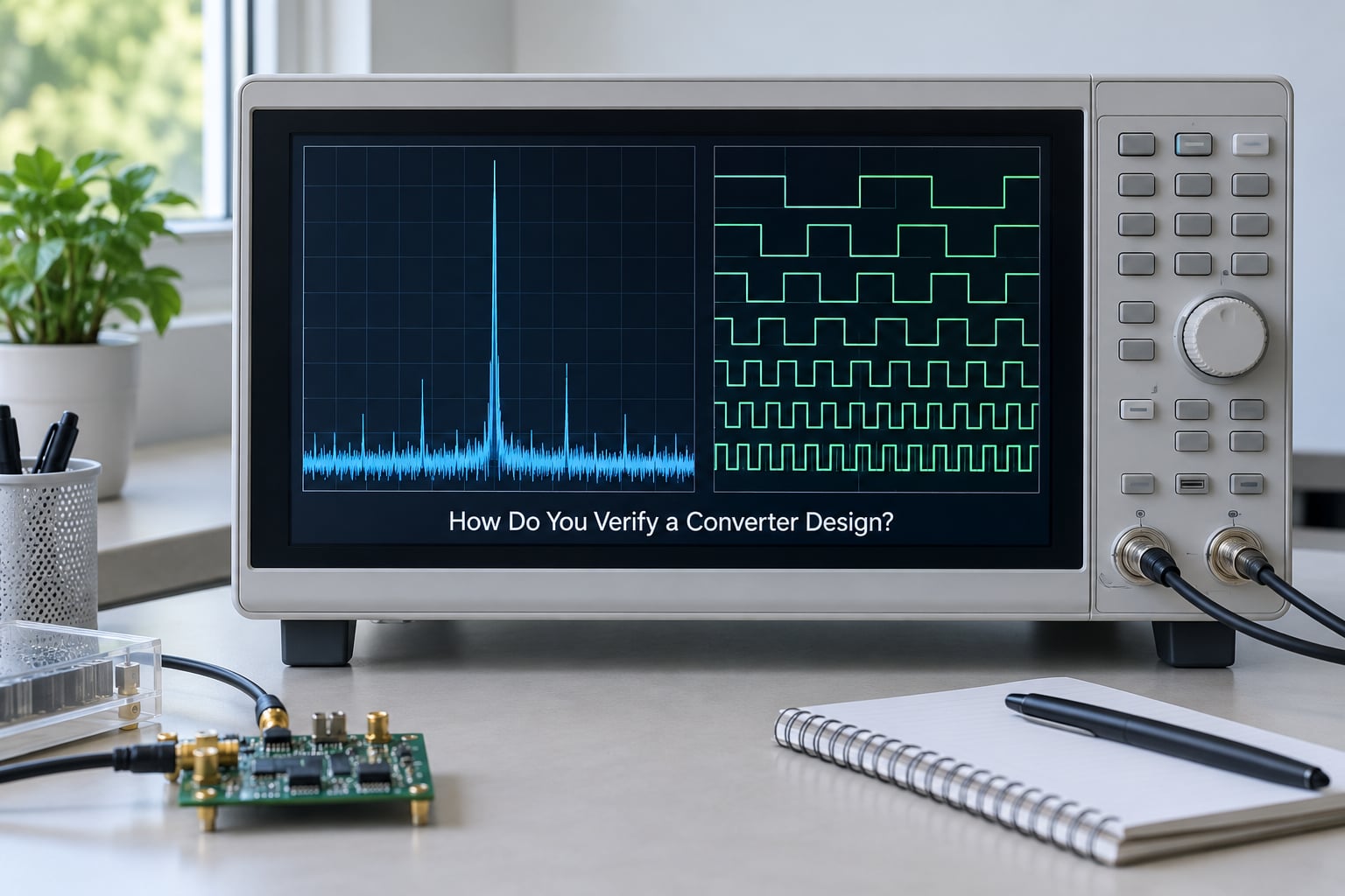
Verification splits into static and dynamic, and both matter before tape-out because the failures look different.
Static testing establishes DC accuracy. A slow ramp or a histogram over a driven input produces the transfer function, and from it you extract offset error, gain error, INL, DNL, and missing codes. Run it across process corners, supply corners, and temperature, because analog accuracy drifts faster than the digital logic around it. Monte Carlo simulation catches mismatch effects that a corner sweep can miss.
Dynamic testing needs a coherent sine input at a rational fraction of the sample rate, so the record length holds an integer number of cycles and the FFT does not smear energy across bins. From that record you compute SNR, SINAD, THD, SFDR, and ENOB, and the spurs on the plot point straight at their causes: a spur at the sample-rate harmonic suggests clock or layout coupling, while a cluster near full scale suggests nonlinearity or code-dependent glitch.
Also check the parts that never show up in a table. Glitch energy at code transitions matters for a DAC feeding a mixer or a reconstruction filter. Startup behavior matters if the converter powers up before its reference settles. Latency should be measured at the pins, not trusted from the block diagram, and corner conditions should include reference tolerance and supply noise rather than nominal values only.
Simulation has a real place. Analog and digital co-simulation catches clock domain crossing errors, interface protocol bugs, and calibration logic problems long before layout, but it will not model parasitic coupling, package effects, or reference noise with enough fidelity to sign off on SNR. Treat simulation as verification of the digital half and as a design aid for the analog half, and plan bench measurement regardless.
What Are the Most Common ADC and DAC Design Mistakes?
- Quoting nominal resolution. A 16-bit part with 13 bits of ENOB does not deliver 16-bit results. Set the ENOB target first and let resolution follow.
- Ignoring the full-scale range. A 0 to 5 V sensor into a converter expecting 0 to 3.3 V loses range or clips. Check the input range against the signal before the bit count.
- Under-filling the antialias filter. The transition band has to fit between passband and Nyquist, and the filter needs flatness in the passband. Cheap filters destroy accuracy.
- Sharing a reference with digital logic. Reference noise and supply ripple show up directly as SNR loss.
- Under-budgeting clock jitter. Measure jitter at the converter pin, not at the PLL output.
- Ignoring latency. Pipeline converters add tens of cycles. In a control loop that phase delay belongs in the loop analysis from day one.
- Comparing datasheets under different conditions. SNR at minus 5 dBFS with a 0.5 Vpp input is not comparable to SNR at full scale. Check the test conditions, the frequency, the supply, and the temperature for every number you compare.
Frequently Asked Questions
Is a higher-resolution ADC always better for a chip design?
No. Resolution costs area, power, and often latency, and it only helps if the rest of the signal chain can feed the converter that much accurate information. A noisy sensor or an unfiltered input will not produce more accurate digits from a higher-bit part. Decide the ENOB you need from your error budget first, then choose the smallest resolution that reaches it, because the extra bits usually cost more than the extra performance returns.
How do I calculate the minimum sample rate for an ADC?
The minimum is twice the highest frequency you need to capture, which is the Nyquist rate. In practice you sample faster than that because the antialias filter needs a transition band, and because oversampling lowers quantization noise density after digital filtering. Many designers sample at four to eight times the signal bandwidth for exactly those two reasons. Remember that each doubling of rate also doubles power in most architectures.
What is converter latency and why does it matter?
Latency is the time from the sampling instant to when a valid output code is available. A SAR converter is typically under two cycles, while a pipeline converter runs to tens of cycles and a filtered delta-sigma to milliseconds. It matters wherever the loop closes through the converter: in motor control, feedback regulation, or any digital correction, added delay is phase shift that can destabilize a system that was stable on analog accuracy alone.
Should analog and digital converter grounds be connected together?
They have to meet somewhere, because current returns to the supply through both, and separating them completely leaves no return path. The point is to control where they meet. On a board, use a single low-impedance connection point under the converter and keep analog and digital return currents on their own planes. In an IC, that means separate power domains, a controlled connection inside or beneath the converter, and floorplanning that keeps high-activity digital logic away from the analog block.
Can ADC and DAC performance be verified adequately in simulation?
Simulation verifies the digital side well: interface protocols, clock domain crossings, calibration logic, and register behavior. It does not carry enough fidelity for sign-off on SNR or SFDR because it cannot model parasitic coupling, package effects, reference noise, or supply ripple through the layout. Use co-simulation to de-risk the digital half and to sweep architecture choices early, then plan bench measurement with code density, histogram, and FFT tests across corners before you commit to tape-out.
Conclusion
The useful part of adc and dac basics for chip designers is not the definitions, it is the order of decisions. Write down the analog bandwidth, the required accuracy as an ENOB and INL target, the sample rate, the power and area budget, the latency you can tolerate, and the digital interface before you look at any architecture. Those six lines eliminate most candidate parts on their own.
After that, match architecture to rate: SAR for moderate speed and low power, pipeline or time-interleaved for wideband, delta-sigma for narrow-band high resolution. Then protect the result with a clean reference, split supplies, controlled grounding, and a real antialias or reconstruction filter. Verify statically with histograms and ramps, dynamically with a coherent FFT, and at the corners. That sequence is what turns a datasheet number into a working converter in your silicon.