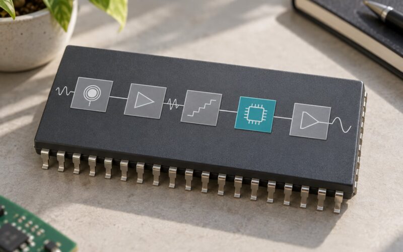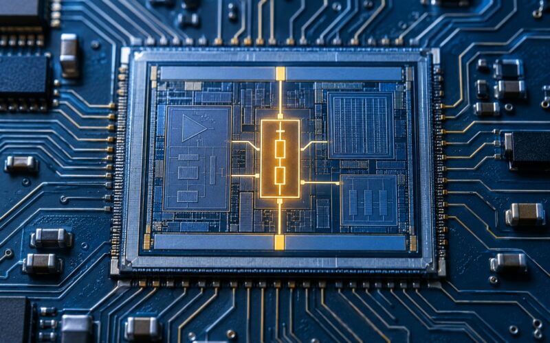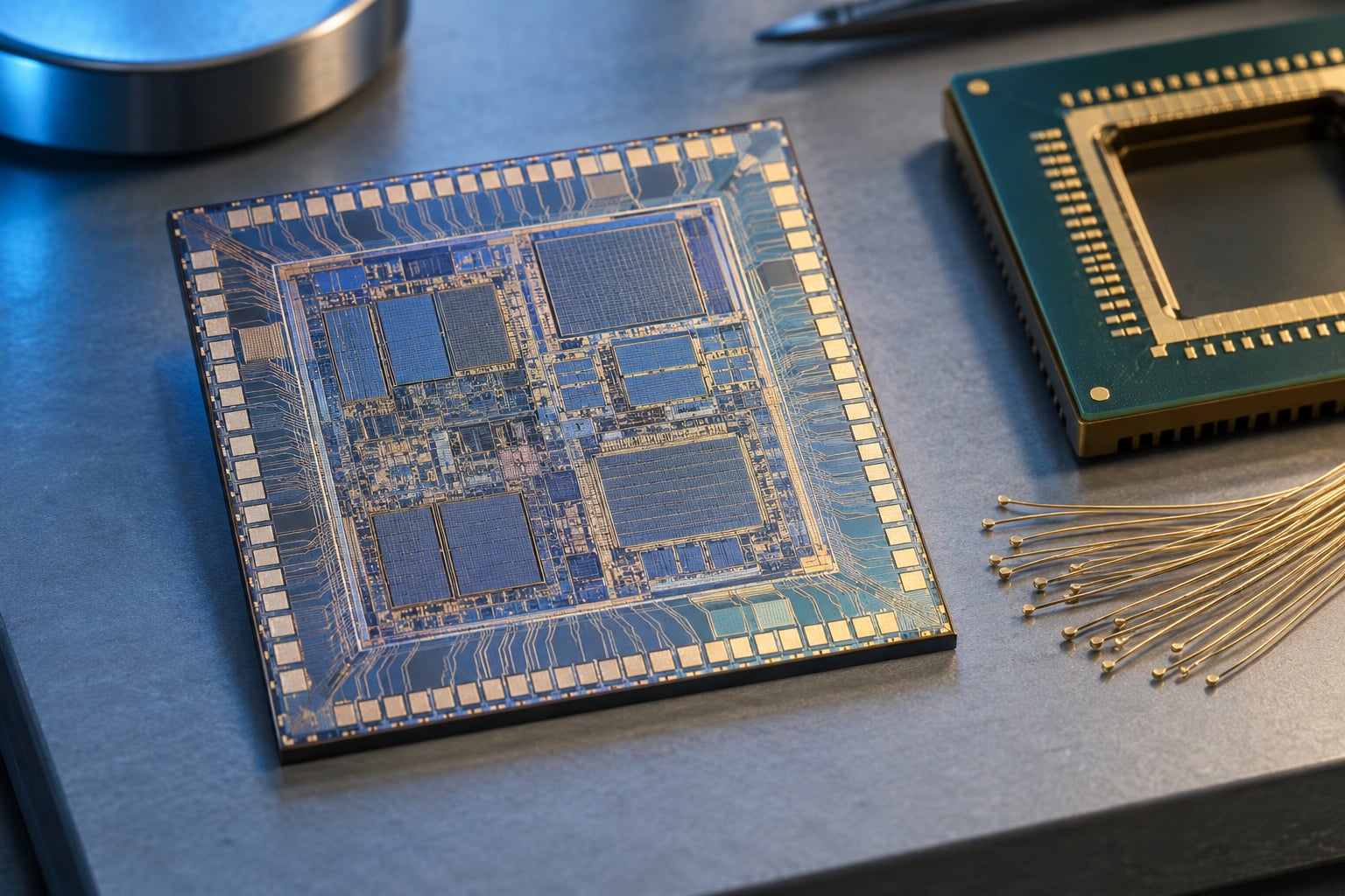
An I/O library is a pre-characterized set of input and output cells that a designer places around the edge of a die so the chip can talk to the outside world safely. It supplies the pad cells, ESD protection, level shifters, power and ground pads, timing models and layout views that a foundry or IP vendor has already verified in silicon.
The term collides badly in search results, so it helps to pin down what this article means. Here, an I/O library is a physical design library of cells at the die perimeter. It is not the same thing as a software I/O library, and it is not a general-purpose chip I/O driver you program in firmware.
Table of Contents
- IO Libraries in Chip Design Explained
- How is an I/O library different from a standard-cell library?
- What Is an IO Library?
- IO device vs IO cell: two different things
- Why core cells cannot do the job
- What Files and Views Are Included in an IO Library?
- How IO Libraries Fit into the Chip Design Flow
- Where the pad ring actually changes the floorplan
- How Do Designers Choose the Right IO Cell?
- Representative cases
- How Do You Use an IO Library in RTL and Verification?
- What verification needs to cover
- What Are the Main Benefits and Limitations?
- Frequently Asked Questions
- Are I/O libraries the same as standard-cell libraries?
- Why are I/O libraries specific to a foundry and process node?
- How are I/O cells used in RTL designs?
- What should I do if the foundry I/O library is not available?
- How do I/O libraries affect chip power, area, and performance?
- Can engineers modify I/O cells for a custom interface?
- Conclusion
IO Libraries in Chip Design Explained
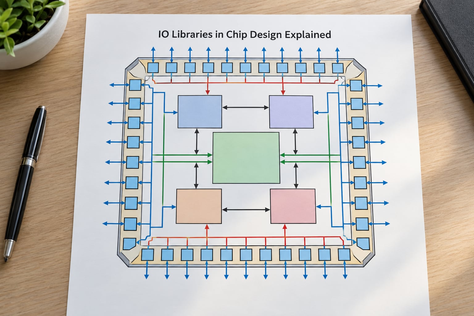
Every silicon chip has a core that works at a low, tightly controlled voltage, and an edge that has to survive whatever the outside world throws at it. An I/O library is the collection of verified cells that bridges that gap. It supplies the input buffers, output drivers, bidirectional pads, power and ground pads, ESD clamps, level shifters and corner spacers that make up the pad ring.
It also supplies everything the tools need to use those cells. That means Verilog simulation models, Liberty timing and power data, LEF layout abstracts, GDSII geometry, a pad frame layout, and a datasheet with the numbers the design will be judged on. A design team can take a qualified library and build a complete, spec-compliant chip interface without ever drawing a pad transistor.
How is an I/O library different from a standard-cell library?
A standard-cell library is what builds the core: NAND gates, inverters, flip-flops, adders. Those cells are optimized for speed, density and low leakage at one narrow voltage range, and they are far too small and too fragile to connect to a package pin. An I/O library is physically much larger per cell, tolerates a wider voltage range, takes the ESD hit, and drives real load. The two libraries are used together on the same die and are almost always delivered separately.
What Is an IO Library?
An I/O library, also called a pad library or pad frame library, is a set of pre-designed and pre-characterized cells used to build the input and output interface of an integrated circuit. Its cells are placed around the die edge, wired to the core netlist, and connected to package pins through bond wires or flip-chip bumps.
Each cell has a job, and the taxonomy is worth learning because almost every pad-ring question reduces to picking the right one. The usual cast includes digital input buffers, output drivers and bidirectional pads, plus supporting cells for power, protection and mechanical fill.
| Cell type | What it does | Typical use |
|---|---|---|
| Input buffer | Conditions a pad signal and presents it to core logic | Buttons, straps, sensor inputs |
| Output driver | Sources or sinks current to a defined load | Driving a board-level net |
| Bidirectional pad | Switches between input and output with tri-state | GPIO, external bus shared lines |
| Power and ground pad | Feeds a supply rail to the die, often through a bond wire or bump | Core and I/O supply distribution |
| Core supply cell | Isolates the I/O supply rail from the core rail | Multi-supply designs |
| ESD clamp and trigger | Drains an electrostatic discharge to a rail | Every externally exposed pin |
| Level shifter | Translates between two voltage domains | Core voltage to I/O voltage |
| Termination | Adds a series or pull resistance to damp edges | High-speed or long lines |
| Schmitt trigger | Hysteresis on a slow or noisy input | Clock inputs, debounced keys |
| Isolation cell | Blocks a signal path between power domains | Power-gated sections |
| Bus keeper or retention | Holds a defined level when a driver goes away | State preserved across power gating |
| Corner spacer | Square-off the die corner geometry | Mechanical fit at the four corners |
| Filler and decap cells | Fill empty pitch, add decoupling capacitance | Pad row density and IR drop |
| Diode breaker | Protects a supply rail from forward conduction | Rail isolation and hot-plug behaviour |
| Test pad | Gives DFT or boundary-scan access at the die edge | Scan chains, probe access |
Many libraries group these into a smaller number of families: general-purpose IO, special-function high-speed IO, analog and mixed-signal pads, power and ground pads, and test IO. Synopsys, for example, describes its GPIO library as including supply cells, corner spacers, diode breakers and terminators, which is the standard support set you would expect to see around a complete pad ring.
IO device vs IO cell: two different things
An I/O device is a functional block such as a UART, an SPI controller or an I2C master. It is logic that happens to live near the edge of the chip and is what firmware calls a peripheral. An I/O cell, or pad cell, is a single physical library element inside the I/O library that connects one pad to the core. A CPU is not an I/O device either. It is a block of general-purpose logic that many I/O devices talk to, and it may contain I/O cells of its own.
Why core cells cannot do the job
Core standard cells run at a narrow voltage, are sized for minimum capacitance, and carry no protection. Push a core inverter onto a pin and you get no ESD survival, no ability to source or sink the milliamp-class current a board net needs, no tolerance for the voltage excursions found outside the die, and a pad geometry too small for a bond wire. That is why an I/O library exists as a separate, separately qualified deliverable.
What Files and Views Are Included in an IO Library?
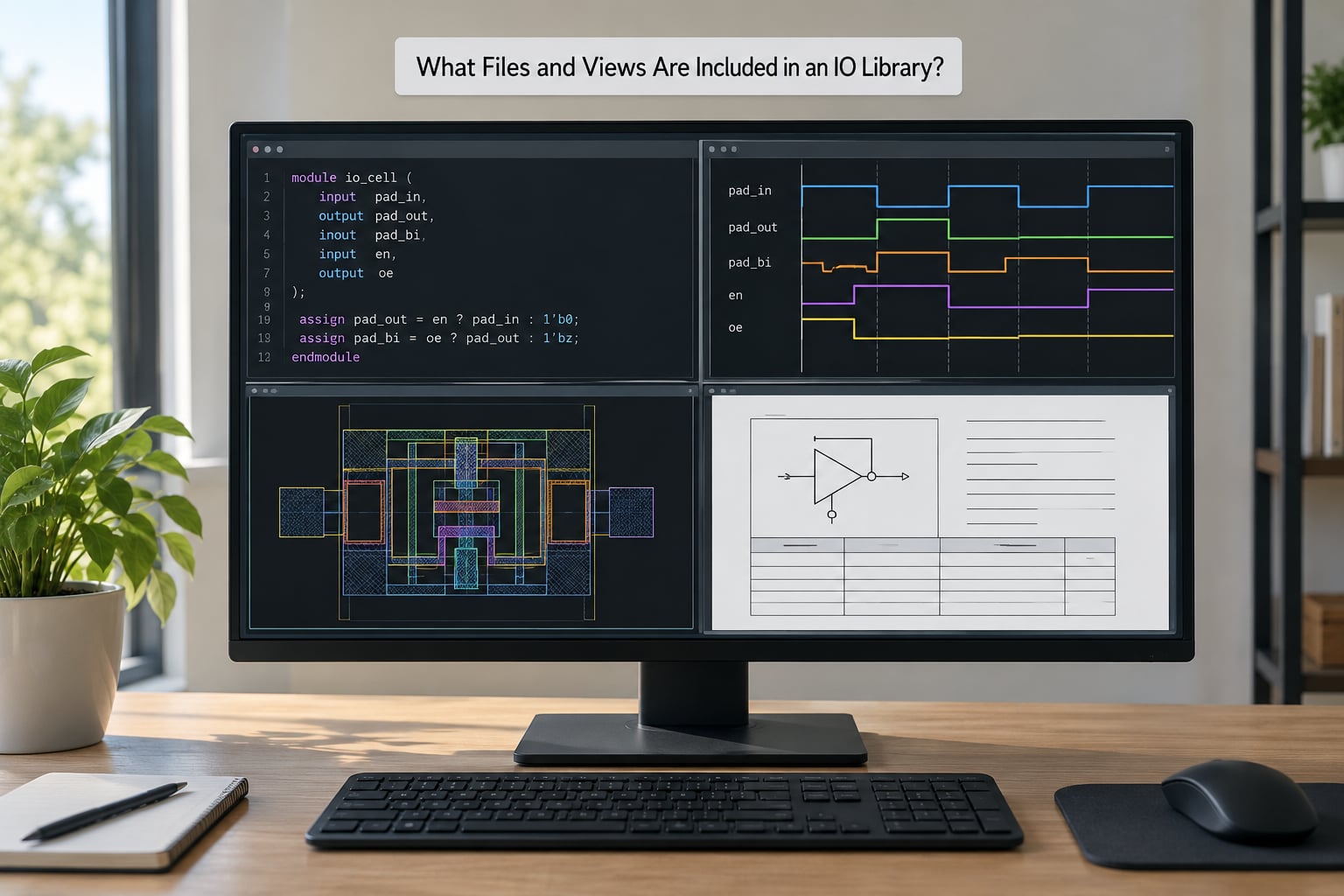
The library arrives as a set of views, and each view answers a different tool’s question. If you know which file to open for which job, evaluating a library takes minutes instead of a day.
| View or file | Format | What the tool uses it for |
|---|---|---|
| Simulation model | Verilog or VHDL | RTL simulation and gate-level simulation |
| Timing and power library | Liberty .lib | Timing, power and leakage analysis, characterization corners |
| Layout abstract | LEF, and DEF for the pad frame | Placement, routing and physical verification |
| Layout geometry | GDSII or OASIS | Signoff DRC, LVS, mask generation |
| Pad frame layout | GDSII plus a floorplan file | Instantiating a prebuilt ring instead of building one |
| Black-box declaration | Liberty or Verilog | Lets synthesis and STA treat a pad as a timing element |
| Annotated delay | SDF | Gate-level timing back-annotation |
| Schematic symbols | Vendor symbol library | Editing schematics when new cells are added |
| Datasheet | Drive strength, slew, leakage, ESD and latch-up numbers | |
| Qualification reports | ESD, latch-up and characterization evidence | |
| Design rules and DRC deck | Foundry deck | Checking pad geometry and spacing |
Two things trip up newcomers. First, a Verilog model is often a behavioural or black-box model, so simulation tells you the logical function but not the electrical reality. Second, the numbers that matter most for signoff, drive current, slew rate, leakage and ESD levels, live in the datasheet and the Liberty file, not in the model. Read both.
The relationship to the rest of the kit matters too. The I/O library is normally delivered inside the process design kit, or PDK, alongside the standard-cell library, the memory compilers and the design rules. A licensed GPIO IP library is a separate purchase that plugs into the same flow but covers a different set of nodes and applications.
How IO Libraries Fit into the Chip Design Flow
An I/O library touches nearly every stage of chip design, but it enters the flow at the top and constrains it all the way down. The order below is the sequence a design team actually works in.
- Architecture. Interface requirements become a pin count, a voltage-domain plan and a package ballout. This is the point where you count how many pads you need and what each one does.
- RTL design. The pad cells are instantiated in the top-level netlist. The same cell names appear in the schematic, so a new cell with no symbol is a real problem.
- Synthesis. The tool reads the Liberty file. Pads are usually instantiated rather than inferred, but their timing arcs still constrain the paths behind them.
- Floorplanning. The pad ring is built first, because it fixes die dimensions, aspect ratio and the power grid that everything else connects into. The padframe supplied with the library can be instantiated as a prebuilt block at this stage.
- Place and route. Pad rows are placed along the die edge, core rows are placed inside, and the power grid is stitched to the power and ground pads. Commands such as addRing and addStripe in Innovus, or the equivalent in other tools, are used here.
- Signoff. Static timing, power integrity including IR drop, DRC, LVS, signal integrity and ESD review all read the library views.
- Packaging and test. The pad pitch and pad order you committed to must match the package. Boundary scan or DFT access runs through the pad ring, so pad assignment affects test coverage.
Where the pad ring actually changes the floorplan
The ring is a fixed-width frame around a flexible core, and it is a large fraction of a small die. One published floorplanning example takes a 500k standard-cell design and arrives at a 1.99 mm by 1.99 mm die once a 150 micrometre I/O ring is added on all sides. Widen the ring, add more power pads for IR drop margin, or move to a finer pad pitch, and the die grows with it. On a wafer, die area is the single biggest lever on how many good die you get.
Pad pitch is constrained from the outside in. The bond pad opening, the wire or flip-chip bump rules, and the package ball pitch all impose a floor on how closely you can pack pads, which in turn forces a minimum ring width.
How Do Designers Choose the Right IO Cell?
Choosing an I/O cell comes down to matching the cell’s electrical rating to the interface you actually have. Work through these criteria in order, and most selections fall out quickly.
- Voltage standard. What voltage does the far end of the line sit at? 1.8 V, 2.5 V, 3.3 V or 5 V determines which family of pads is even legal, and whether you need a level shifter between the core supply and the I/O supply.
- Direction. Input, output or bidirectional. Bidirectional pads cost more area and power because they carry both a driver and a receiver.
- Drive strength and load. Match the cell’s IOH and IOL to the capacitance and the line length you drive. Oversizing burns power; undersizing slows the edge and risks timing failures downstream.
- Slew rate. Slower edges radiate less and cross-talk less, which matters on a long unshielded net. Faster edges are needed for short nets and high-rate interfaces.
- Speed and protocol. A general-purpose LVCMOS pad is not a DDR pad, and neither will drive a multi-gigabit serial link. High-speed IO families come with their own impedance, reference clock and termination requirements.
- Leakage and power. Bidirectional and high-speed cells idle at real static current. On a low-power part, dozens of pads can dominate the leakage budget.
- Area and pad pitch. The cell width has to fit the row pitch, and the row pitch has to fit the package.
- ESD and latch-up requirement. Consumer parts, automotive parts and parts sold into industrial environments carry different qualification bars.
- Process node. A library is built and qualified for one process. A cell qualified at 90 nm means nothing at 7 nm.
Representative cases
A UART transmit pin is a modest case: 3.3 V output, low drive, slow edges, ordinary ESD. A GPIO on a battery-powered sensor node is a power case, where a failsafe output and low leakage matter more than drive. A DDR memory interface needs the high-speed IO family with a Schmitt-triggered clock input and controlled slew. A clock input pad wants a Schmitt trigger, and nothing else. A SerDes lane is not a pad choice at all, it is a PHY with a defined impedance and reference clock, sitting behind a small number of IO cells.
Analog and mixed-signal pads come with their own rule set. They need guarding, separation from switching digital pads, and usually their own quieter supply. A recurring question on engineering forums is whether an analog front end should instantiate a pad library in a custom flow. The usual answer is yes for the digital interface, and for the analog pins use the analog pad family with the separation rules the datasheet specifies, rather than improvising.
How Do You Use an IO Library in RTL and Verification?
In RTL, an I/O cell is an ordinary module instantiation. You bring the pad signal in, pass it to the core, and route core signals out to the pad, with separate supplies where the library requires them.
module uart_tx_pad (
  input  wire       core_clk,
  input  wire       core_rst_n,
  input  wire       tx_data,
  output wire       tx_valid,
  inout  wire       uart_tx,     // pad-level net to the package pin
  inout  wire       vdd_core,
  inout  wire       vdd_io
);
  // Instantiated from the foundry I/O library, not written by hand
  IOPAD_X8N uart_tx_i (
    .pad(uart_tx), .core(tx_data), .core_clk(core_clk),
    .core_rst_n(core_rst_n), .out_valid(tx_valid),
    .vdd_core(vdd_core), .vdd_io(vdd_io)
  );
endmodule
The names are placeholders, but the pattern is not. The cell name has to exist in both the Verilog view and the Liberty view, and its symbol has to exist in the schematic library, or the cell will not survive editing.
What verification needs to cover
- Functional simulation. Run the pad model against the RTL, including reset, tri-state and contention cases where two drivers share a net.
- Timing exceptions. Pad timing is often constrained through the library rather than with a hand-written exception, so check how the cell is characterized in the Liberty file before adding set_false_path.
- Corner testing. Simulate across worst-case, best-case and typical process corners with slow and fast timing, because the pad’s own delays move with them.
- X-propagation. Uninitialized pad nets and bus keeper behaviour are a classic source of X’s that survive to gate level. Check them deliberately.
- Power-off behaviour. If a pin can be driven externally while its supply is down, the failsafe path must be verified, not assumed.
Keep functional and electrical signoff separate in your head. Simulation tells you the pad does what you wired it to do. Electrical signoff, using the datasheet numbers, Liberty data, power integrity and DRC results, tells you it survives contact with the real world.
What Are the Main Benefits and Limitations?
The case for using a qualified I/O library is mostly about risk and schedule. The cells are already designed, characterized and proven in silicon, the ESD and latch-up work is done, and the timing and power data is trusted by the tools. For a team trying to hit a tapeout date, that removes a large block of work that is easy to underestimate.
The predictable interface is the quieter benefit and probably the bigger one. Every pad behaves the way the datasheet says, so a design review can reason about the edge without simulating a transistor. Reusing a verified library also means the same interface can be carried from one project to the next, which matters for anyone building a family of parts.
The limitations are real, though. Licensing is a cost, and for a foundry PDK library that cost is already sunk while a licensed vendor GPIO library is a separate line item with its own lead time. The library is locked to a process, so a node change means re-qualification. Simulation models are frequently black boxes, which means some behaviour only appears at gate level or on silicon. Customization is limited, because modifying a qualified pad cell takes you out of the qualification envelope. And the foundry design rules for the pad area are not optional.
Foundry PDK I/O is the sensible default when the part is a conventional SoC on a mainstream node, because it is free with the process, fully characterized, and matched to the design rules by construction. Licensed vendor GPIO IP earns its place when the design needs coverage across several nodes, more functionality than the PDK offers, an automotive qualification the foundry library does not carry, or a schedule where waiting for the foundry library is the bigger risk. Ask for the qualification package, the maturity level, and the supported process list before either option goes on a purchase order.
Frequently Asked Questions
Are I/O libraries the same as standard-cell libraries?
No. A standard-cell library builds the core with gates, flip-flops and adders optimized for speed and density at one narrow voltage. An I/O library holds the perimeter cells: input buffers, output drivers, bidirectional pads, power and ground pads, ESD clamps, level shifters, corner spacers and terminators. The two are used on the same die and are normally delivered separately, with the I/O library arriving inside the process design kit.
Why are I/O libraries specific to a foundry and process node?
The cells are drawn, characterized and qualified on one process. Their ESD structures, device physics, drive capability and leakage all depend on that process, and a pad qualified at 90 nm says nothing about a pad at 7 nm. Foundry design rules also govern pad geometry and spacing, so a library from another process will not pass DRC. That is why every I/O library is node-specific and tied to its foundry.
How are I/O cells used in RTL designs?
They are instantiated as modules in the top-level netlist, much like a macro. A bidirectional pad is declared as an inout, tied to its supply rails, and connected to the core signal it serves. The cell name must exist in the Verilog view, the Liberty view and the schematic symbol library, or the design will not close cleanly. Tools then read the pad timing from Liberty during synthesis and signoff.
What should I do if the foundry I/O library is not available?
Ask the foundry for the release schedule and an interim cell list, because a late library forces late pad decisions. In parallel, evaluate a licensed vendor GPIO library that covers your process, and check its maturity level and qualification package. A workable fallback is a reduced pad set: fewer voltage domains, fewer analog pads, and no optional features until the full library lands.
How do I/O libraries affect chip power, area, and performance?
They affect all three. Area grows because pads are much larger than core cells and the ring adds width on four sides. Power rises from static leakage in bidirectional and high-speed pads, plus the switching load of driving external capacitance. Performance is mostly a timing question: an undersized driver slows the edge and can break downstream hold or setup, while an oversized one wastes power. Pad pitch and package rules cap how tightly you can pack them.
Can engineers modify I/O cells for a custom interface?
Technically yes, physically rarely wise. Editing a qualified cell invalidates its characterization, its ESD and latch-up results, and any foundry signoff that depended on it. Most teams stay inside the qualified cell set and build the custom behaviour around the pad instead. A genuinely custom pad usually means a custom IO design project with its own characterization and qualification, which is a different commitment from writing RTL.
Conclusion
An I/O library is the verified set of cells and views that turns a die edge into a working, protected chip interface. It supplies the pads, the ESD and latch-up protection, the power and ground distribution, and the models the tools need, and it removes a large block of design work that is genuinely hard to redo late in a program.
If you are new to this, do three things in order. First, fix the process node and the package, because both constrain everything about the pad ring. Second, get the foundry-approved I/O library, or a licensed vendor library if the foundry timing does not work, and read its datasheet and qualification report before writing a line of RTL. Third, map each interface requirement to a specific cell, and check the mapping against the pad count, the package ballout and the supply plan you have committed to.
Get those three right and the rest of the flow mostly takes care of itself.