Flip Chip Packaging Explained (2026): Process, Benefits
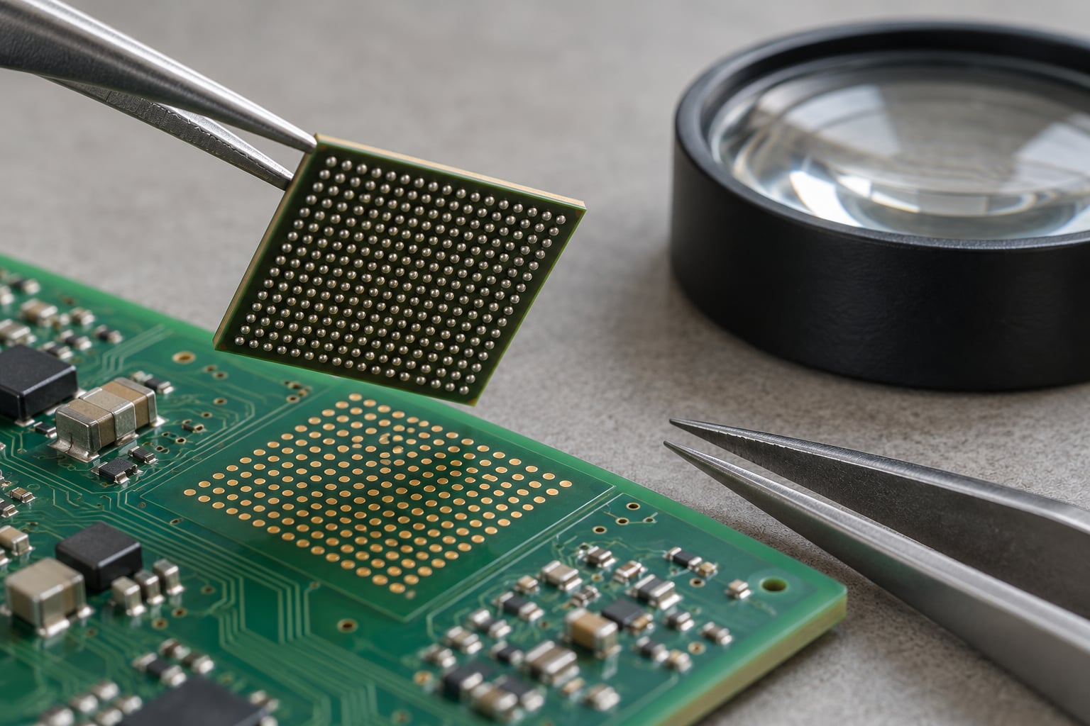
Flip chip packaging is a way of connecting a bare semiconductor die to a substrate or circuit board: the die is turned face-down so … Read more

 Dalton Briggs
Flip chip packaging is a way of connecting a bare semiconductor die to a substrate or circuit board: the die is turned face-down so … Read more
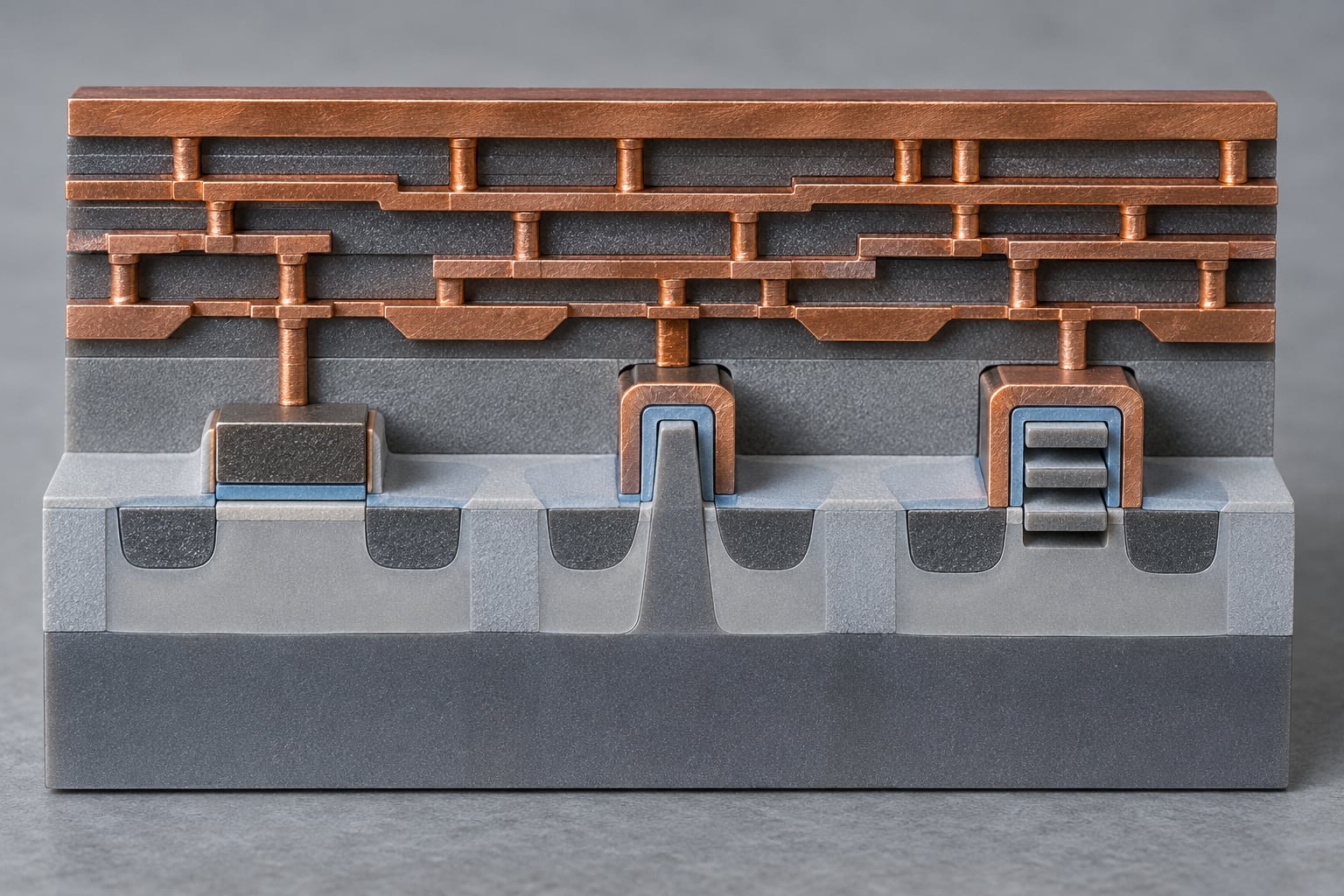
Here is the short answer: transistors shrink because lithography keeps printing smaller features, and for decades each generation cut key dimensions by roughly 0.7x … Read more
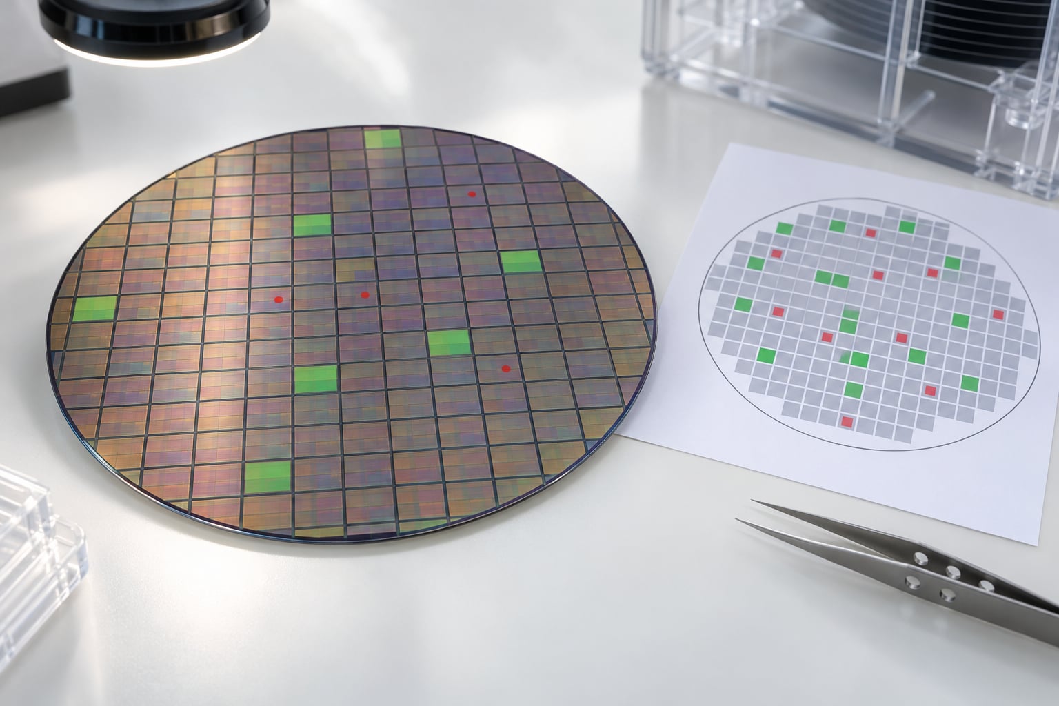
The short version of how semiconductor yield is calculated is one division: the number of functional (good) dies divided by the total number of … Read more
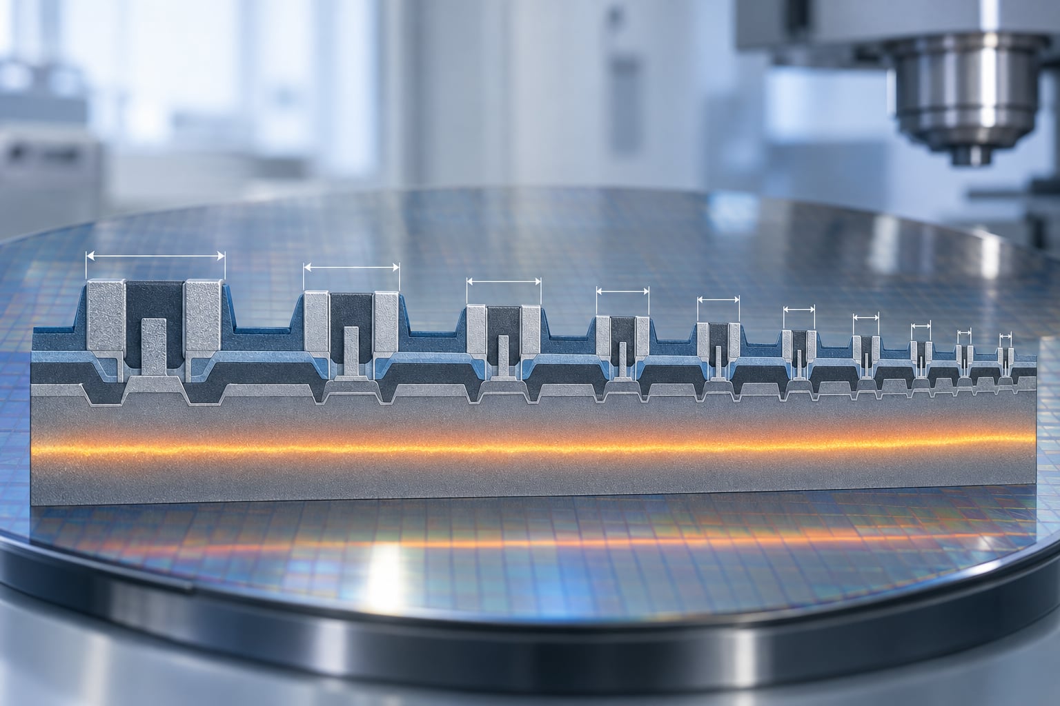
Dennard scaling is a law from a 1974 IEEE paper that says transistor dimensions, supply voltage and doping can be shrunk together so that … Read more
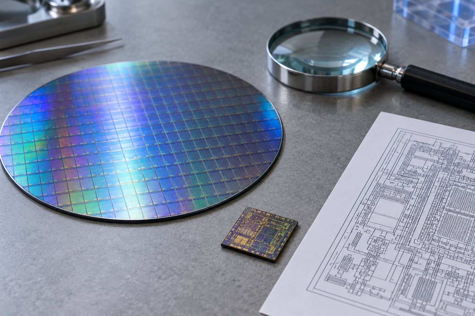
Moore’s Law is the observation, first published by Intel co-founder Gordon Moore in 1965, that the number of transistors you can fit on a … Read more

A FinFET is a three-dimensional transistor in which the gate wraps around a thin, vertically standing silicon fin on three sides instead of controlling … Read more
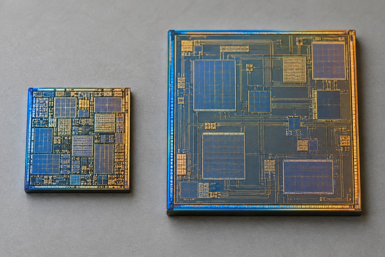
Choosing between the 3nm and 5nm process nodes comes down to one question: does the smaller node buy enough performance-per-watt or logic density to … Read more
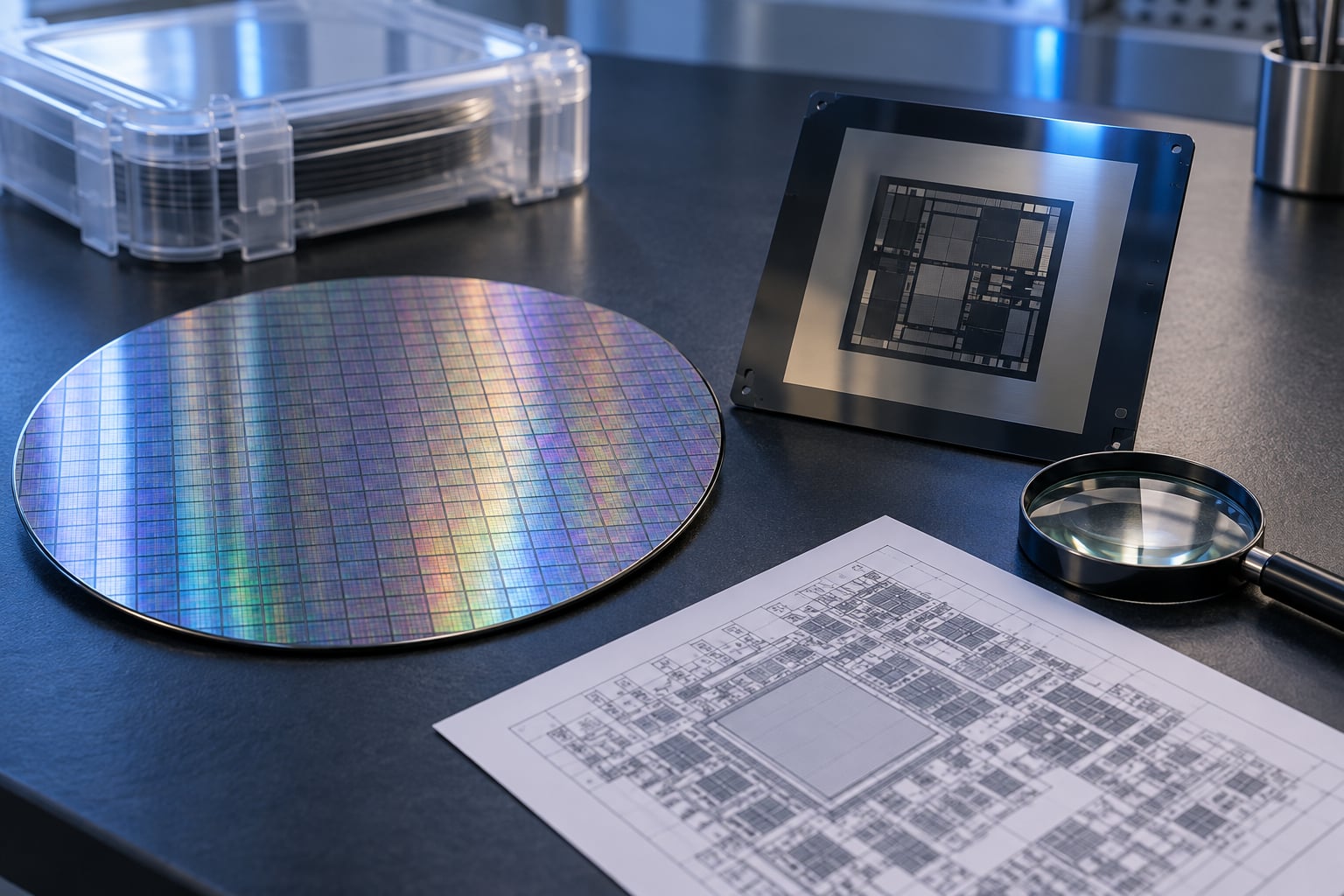
A semiconductor foundry is a company that manufactures chips other companies designed. It takes a finished layout file, prints that layout onto silicon wafers … Read more
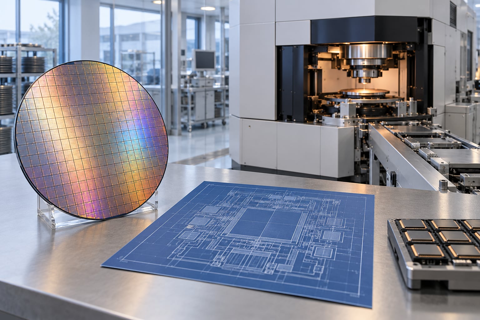
A foundry builds chips that other companies designed, a fabless company designs chips but owns no factory, and an IDM does both under one … Read more
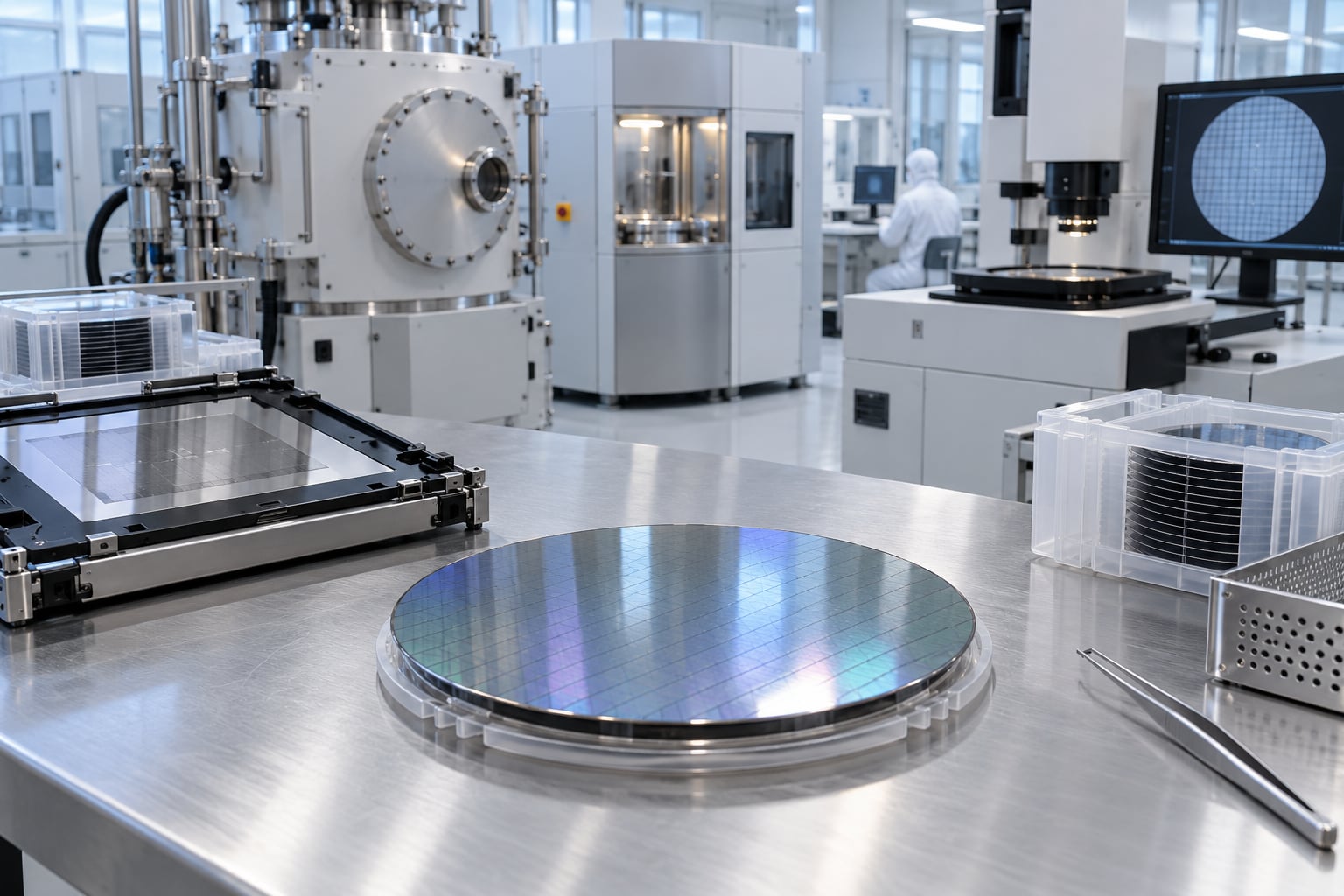
Here is the short version: wafer fabrication is the process of building microscopic transistors and wiring layers onto a polished silicon wafer, using repeating … Read more