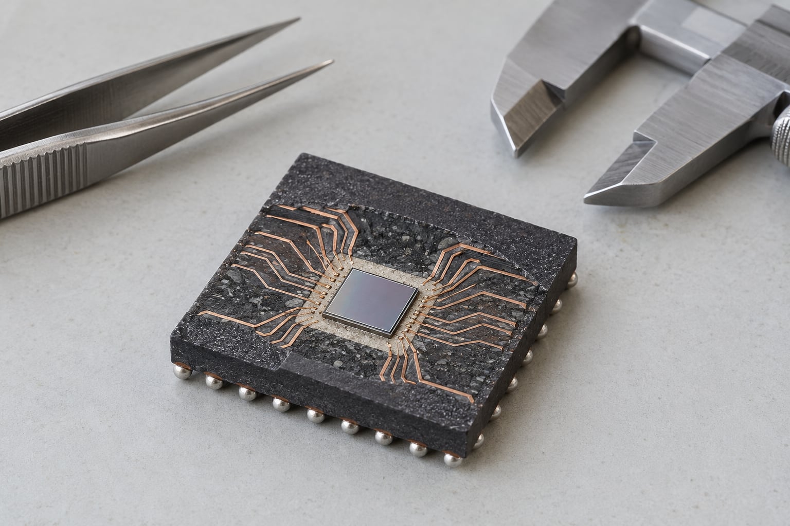
Fan out wafer level packaging (FOWLP) is a semiconductor packaging method that embeds bare die in mold compound and routes every connection outward through a copper redistribution layer, so the finished package needs no separate substrate and is barely larger than the die itself.
That single change — dropping the organic substrate — is why fan out replaced wire-bonded packages in smartphone application processors, RF front-end modules and 5G millimetre-wave antenna-in-package designs. If you are evaluating a package for a fine-pitch device, the parts that matter are the process flow, the RDL line and space, and the failure modes nobody puts on the datasheet. This guide walks through all of it.
Table of Contents
- What Is Fan Out Wafer Level Packaging?
- How Fan Out Wafer Level Packaging Works
- What Is the Difference Between Fan-In and Fan-Out WLP?
- What Are the Main Fan-Out WLP Architectures?
- Single-die and known-good-die fan-out
- Chip-first face-up flows
- RDL-first and die-last flows
- Multi-die fan-out
- Panel-level fan-out (FOPLP)
- Fan-out as an interposer substitute
- What Materials Are Used in Fan-Out Wafer-Level Packaging?
- Why Choose Fan-Out Wafer-Level Packaging?
- What Are the Limitations and Manufacturing Challenges?
- How Does Fan-Out WLP Affect Design and System Integration?
- Where Is Fan-Out Wafer-Level Packaging Used?
- Frequently Asked Questions
- Is fan-out WLP the same as flip-chip packaging?
- What is the main function of the redistribution layer?
- Does fan-out wafer-level packaging support very large semiconductor dies?
- How are devices tested before and after fan-out packaging?
- Is fan-out WLP always cheaper than organic substrate packaging?
- Conclusion
What Is Fan Out Wafer Level Packaging?
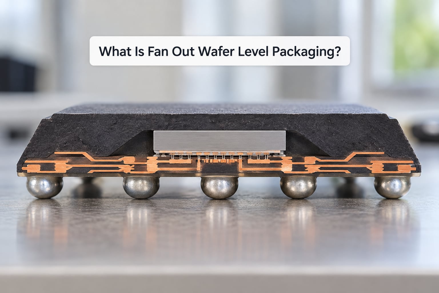
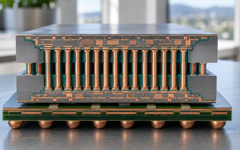
Fan out wafer level packaging, also written fan-out WLP, FO-WLP or FOWLP, packages an integrated circuit by molding it into an epoxy mold compound and building fine copper wiring on top of that molded body. The wiring carries the die’s input and output pads to a wider area, which is where the solder balls attach.
In conventional wafer-level packaging (WLP), by contrast, routing is confined to the space inside the die outline. Known in the industry as fan-in WLP or wafer-level chip-scale packaging (WLCSP), that approach works well for small die with modest pin counts and gets awkward the moment you need several hundred connections on a die that is already large.
So the difference between wafer-level packaging and fan-out wafer-level packaging comes down to what happens first and where the routing lives. In standard WLP, the wafer is assembled and only then diced into finished packages. In fan-out, the wafer is diced into known-good die first, and the die are reassembled into a new wafer with room around each one.
A few related terms cause confusion. A wafer pack is the older name for a package formed while the die is still on its wafer. A chip attach is the individual die inside a package. Knowing which of these you are discussing saves an afternoon of reading the wrong process flow.
How Fan Out Wafer Level Packaging Works
The whole flow exists to solve one problem: you cannot grow copper wiring beyond the edge of a die. So the die is removed from its wafer, placed in a larger frame, and rebuilt into a bigger object before the wiring is drawn.
1. Dicing. The source wafer is diced into individual die. Because a package that contains a defective die is worthless, this step is normally preceded by wafer-level electrical test so only known-good die move forward. That screening is also why the process carries a yield cost, which we cover later.
2. Placement on a carrier. Each die is picked and placed face-up onto a carrier wafer or carrier panel with a die attach film. The placement pattern is deliberately spaced out so that a rectangular fan-out region surrounds every die — that empty mold compound is the routing area that fan-in does not have.
3. Reconstitution by molding. Liquid or film epoxy mold compound is applied over the carrier and the die, then cured. The carrier, film and compound are stripped away, leaving what industry callers call a reconstituted wafer: die embedded in a solid molded body, each one surrounded by solid material that RDL build-up can later use.
4. Redistribution layer build-up. A seed layer is deposited, then electroplated copper traces are patterned, with a polymer dielectric such as PBO between layers. Successive build-up passes create multiple RDL layers where a single layer cannot carry enough escape routes. Fine lines of roughly 5 to 15 µm are typical for established volume processes.
5. Bumping. Under-bump metal pads are formed on the outermost RDL pads, and either solder balls or copper-pillar-plus-microbumps are attached. This is the electrical and mechanical interface to the printed circuit board.
6. Singulation. The reconstituted wafer is diced into finished packages, sent through final test and inspection, and shipped for board attach.
The result sits in a useful physical range. Finished packages land roughly between 0.3 and 0.6 mm tall, and because the redistribution wiring is only a few micrometres thick, pad pitch drops well below what a wire bond or organic substrate would allow.
What Is the Difference Between Fan-In and Fan-Out WLP?
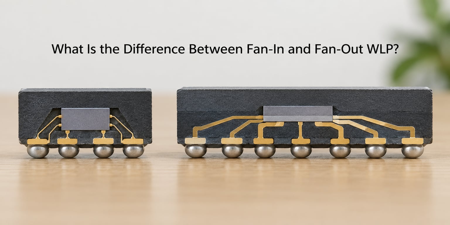
Fan-in is smaller, cheaper and simpler. Fan-out buys you routing area, I/O density and a substrate-free body. The table below is the version I would hand to a product architect choosing between the two.
| Criterion | Fan-in WLP (WLCSP) | Fan-out WLP (FOWLP) |
|---|---|---|
| Routing area | Confined inside the die footprint | Extends into mold compound around the die |
| Package size vs die size | Equal to the die | Larger than the die, but no substrate layer |
| Typical I/O density | Low to moderate, limited by die edge | High, several hundred connections feasible |
| Wafer handling order | Assemble on wafer, then dice | Dice first, then reconstitute into a new wafer |
| Yield exposure | Whole wafer affected by one bad die until final test | Known-good die screening, but each bad die still consumes molding area |
| Cost per package | Lower below a few thousand I/O | Competitive once pin count or volume rises |
| Best fit | Image sensors, small analog and mixed-signal die | Application processors, RF modules, mmWave antenna-in-package |
One practical note. Fan-in’s problem is not cost, it is geometry. A die with 300 pads arranged around its perimeter has nowhere to put the traces, so designers either shrink the pad pitch until routing becomes impossible, or move to fan-out.
What Are the Main Fan-Out WLP Architectures?
Not all fan out is built the same way. The differences show up in flow order and in how many die share one molded body.
Single-die and known-good-die fan-out
The common production architecture places one known-good die per package in a moulding frame sized to the die plus its fan-out margin. Infineon’s eWLB (embedded wafer-level ball grid) technology, commercialised in the mid-2000s for mobile phone chips, established this pattern, and TSMC’s InFO (integrated fan-out) carried it into volume smartphone application processors.
Chip-first face-up flows
In a chip-first flow the die goes down before any wiring. Face-down chip-first puts the die active side toward the carrier, which is compact and short but limits how high the RDL can stack above it. Face-up chip-first exposes the active side for wiring and tolerates taller build-up, at the cost of needing a protective film over the die face.
RDL-first and die-last flows
In an RDL-first, or die-last, flow the redistribution layer is built on a carrier without a die, then die are attached on top from the opposite side. Because the wiring exists before the chip arrives, this flow places the die close to the board — useful for heat spreading — but it caps how much RDL you can stack under the die and needs more back-side wiring to reach everything.
Multi-die fan-out
Several die are placed in one molded body and wired by a common RDL. RF front-end modules routinely integrate two to five die — power amplifier, low-noise amplifier, switch, filter — and advanced smartphone module designs have pushed higher. Passive components such as thin-film inductors and capacitors can be embedded the same way.
Panel-level fan-out (FOPLP)
Panel-level fan-out replaces the carrier wafer with a rectangular panel, moving from 200 mm wafers toward 300 mm and larger panels. The motivation is straightforward economics: more packages per unit of carrier area means less carrier cost per die. The obstacles are panel-level warpage control, handling equipment that was built for round wafers, and inspection tools that assume a chuck of a fixed size.
Fan-out as an interposer substitute
Fan-out entered the industry as a lower-cost alternative to silicon-interposer-based 2.5D and 3D packaging. Where a fine interposer buys very high interconnect density, fan-out buys most of the density at a fraction of the cost and without through-silicon vias. Practitioners generally treat fan-out as the economic alternative to a silicon interposer rather than its equal, and 2.5D interposer parts still win where bandwidth per unit area matters more than cost.
What Materials Are Used in Fan-Out Wafer-Level Packaging?
Every material in the stack earns its place for one of four reasons: structure, conductivity, adhesion, or control of how the package behaves under heat.
Epoxy mold compound. The structural body of the package. It holds the die in position, provides the surface the RDL is built on, and is the main source of warpage because the mould shrinks as it cures.
Polymer dielectric (PBO or similar). The insulating layer between copper RDL layers. Thickness is usually in the single-digit to low-teens micrometre range, and thinner dielectric means more escape density but harder layer-to-layer alignment.
Copper traces and the seed layer. Copper carries signal and power. The seed layer underneath is what makes electroplating uniform; adhesion between copper and dielectric is one of the more common delamination sites in the stack.
Under-bump metal, copper pillars and solder alloys. The bump pad and pillar stack absorbs solder reflow stress, and the solder alloy controls the melting behaviour during board attach.
Underfill and die attach film. The film holds die during moulding and the reconstituted-wafer handling that follows. Underfill fills the gap under the die and spreads heat, which matters on large die.
The board substrate. Not part of the package, but the package exists to land on one. Because the package is substrate-free internally, the printed circuit board becomes the only mechanical support and the main source of board-level strain.
Why Choose Fan-Out Wafer-Level Packaging?
Every benefit traces back to one of two features: no organic substrate, or routing outside the die.
Smaller form factor and low profile. Removing the substrate stack takes roughly 0.3 to 0.6 mm off the finished height and leaves a package footprint close to the die footprint. For a wearable or a phone, that vertical millimetre is what determines whether the device fits at all.
Short electrical paths and low parasitic inductance. A redistribution trace a few micrometres thick is far shorter than a wire bond loop or a substrate trace. Interconnect inductance in established designs stays below about 0.1 nH, which is the figure RF and power integrators care about.
Higher I/O density without growing the die. The fan-out margin is routing area that a fan-in process simply does not have, so several hundred pads can escape from a die that would be impossible to route otherwise.
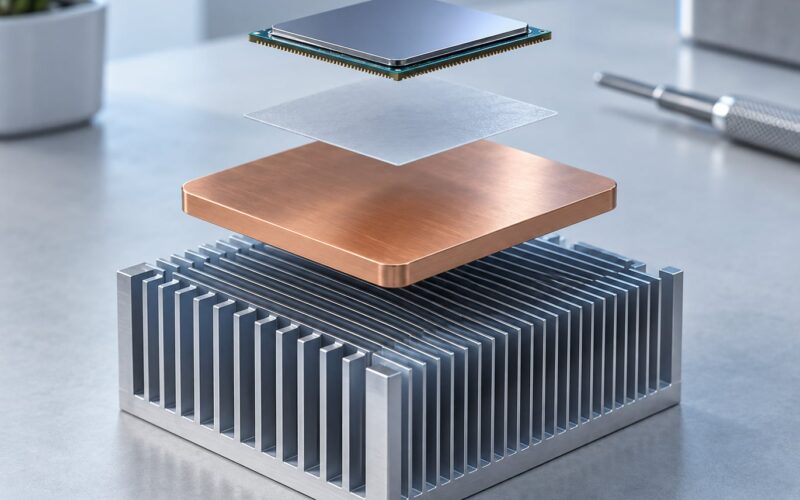
Direct thermal path. With the die backside left exposed, heat from an application processor or power amplifier goes straight to a heat spreader instead of through a stack of substrate, solder and board. That matters most where the die dissipates the most power.
Cost savings at volume. Substrate elimination is the single biggest cost lever, since an organic substrate is usually the most expensive line item in a conventional package. The trade is not free, and the general rule practitioners use is that fan-out pays off somewhere in the one-to-five million units per year range; below that volume, laminate or plastic package costs can still win.
Compatibility with fine-pitch devices. Fine-pitch RF and mmWave parts could not be packaged with wire bonds at all. Fan-out RDL routinely supports the pitch those parts need, which is why antenna-in-package designs exist at all.
What Are the Limitations and Manufacturing Challenges?
The finished package looks simple. The process behind it is not, and a fair account of fan out wafer-level packaging has to name the hard parts.
Mould-compound warpage. Mould shrink during cure and thermal expansion mismatch bend the reconstituted wafer. Large die and large panels are worse, and warpage that is out of spec at singulation becomes a package that does not sit flat on the board.
RDL line and space limits. Fine RDL is what makes fan-out attractive, and it is also the hardest thing to make defect-free. Industry practice generally treats line and space below about 8 µm as the marker of high-end fan-out, and that threshold moves with each process generation.
Die shift during moulding. If a die moves before the compound cures, its pads no longer line up with the RDL built over them. Placement accuracy on the carrier and mould-flow control are the levers.
RDL delamination and cracking. Copper and dielectric have very different expansion behaviour, so copper traces can crack through the dielectric during temperature cycling. Adhesion promoters and matched expansion help; neither eliminates it.
Known-good-die yield loss. Screening to known-good die before reconstitution prevents one bad die from losing a whole package, but every defective die still consumed carrier area and molding compound. On a small die the ratio is bad, on a large die it is better.
Bump and test access. Once the RDL is in place and the package is moulded, most probe points are buried. Wafer-level probe of the RDL is possible before singulation but is harder on a reconstituted wafer than on a flat silicon wafer, and repairs that were routine in substrate assembly are no longer possible.
Inspection. Mould compound is opaque, so defects inside the package are found by X-ray and by cross-section sampling rather than by optical inspection. Metrology on the die surface is well understood; metrology inside a reconstituted wafer is a genuine gap.
Reliability qualification follows the same logic. Temperature cycling and humidity testing target the die attach interface and the RDL stack, while warpage measurement at every temperature step catches what room-temperature inspection misses.
How Does Fan-Out WLP Affect Design and System Integration?
Choosing fan-out is not a packaging decision you can defer to the end. These are the things that change at the design stage.
Pad layout and escape density. Bump pitch and RDL resolution decide how many pads you can escape, and that number is fixed by the process, not by the design. Design rules from the assembly house are the contract, not a suggestion.
Routing rules, not just connectivity. An RDL line that legally fits may still violate the layer’s density or spacing rules. Multi-layer build-up gives more room, at the cost of more dielectric layers and more alignment steps.
Power and ground distribution. Wide planes and via arrays have to be planned into the RDL early. A power net redesigned late usually means a bump layout change.
Signal integrity and impedance. Short interconnects reduce loss, but controlled impedance still has to be engineered, especially on RF traces. This is where electromagnetic co-simulation of the package design matters; commercial tools are marketed specifically for extracting critical nets and running EM-circuit co-simulation on fan-out modules.
Thermal paths. Where the die backside is exposed, the board and enclosure design must actually provide a heat sink. A package that cannot dissipate is a package that throttles.
Test access and known-good-die strategy. How much screening happens before reconstitution, and how much testing happens on the RDL before singulation, directly changes the cost model. Designers need to know which test points the assembly house can reach.
Board footprint. The bump array is irregular and larger than the die. Board layout, via-in-pad requirements and assembly stencil design all follow from that array, so package and board design belong to the same conversation.
The division of labour matters too. IC designers, package engineers and board designers all constrain each other in fan-out, and projects that treat the package as a black box after tape-out tend to discover the limits late.
Where Is Fan-Out Wafer-Level Packaging Used?
Fan-out wins wherever three conditions hold at once: high pin count, tight size limits, and enough volume to amortise the tooling.
Smartphone application processors and baseband. Large pin counts plus a very thin package made this the technology’s first major market, and TSMC’s InFO family built specifically around it.
RF front-end modules. Power amplifiers, low-noise amplifiers, switches and filter die are co-integrated in one molded body, which shortens RF paths between stages and lets several die share a single antenna feed structure.
5G millimetre-wave antenna-in-package. At 28 GHz and 39 GHz, path length is the enemy, so the antenna is placed in the package rather than on the board. Current RDL processes are generally treated as usable up to roughly 40 to 60 GHz.
Automotive radar and sensing. Radar modules need short RF paths, low profile and tolerance for wide temperature swings, which fan-out provides when the die sizes stay moderate.
Network and computing silicon. Network processors and specialised accelerators use fan-out where a package near die size and high I/O density matter more than the absolute pin count a silicon interposer would allow.
Wearables, IoT and security modules. Small form factor drives the choice in wearables and IoT; small die count plus a need for tamper resistance drives it in secure elements and hardware security modules.
The commercial ecosystem runs through TSMC with InFO, Infineon with eWLB, and the OSATs including ASE, Amkor, Samsung and JCET, several of whom have published panel-level fan-out programmes.
Frequently Asked Questions
Is fan-out WLP the same as flip-chip packaging?
No. Both techniques place a die face-down onto a substrate using solder bumps, so the interconnect principle is similar. The difference is what carries the wiring. Flip-chip uses a separate organic or silicon substrate with its own routing layers, while fan-out builds the copper redistribution layer directly into the mold compound around the die, eliminating the substrate entirely.
What is the main function of the redistribution layer?
The redistribution layer is the wiring that carries connections from the die pads to a wider area of the package. Fan-in processes can only route inside the die outline, so pad count is capped by die perimeter. The RDL escapes those pads into the molded region, which is what allows hundreds of connections on a package that is only slightly larger than the die.
Does fan-out wafer-level packaging support very large semiconductor dies?
It works, but large die are harder. Mould shrink and thermal expansion mismatch drive warpage, and warpage grows with die area, which makes singulation and board attachment less predictable. Known-good-die screening also wastes molding area, because every defective die still occupied carrier space before it was rejected, and that waste hurts proportionally more when the die is small. Very large logic die usually stay with organic substrate or interposer packages for these reasons.
How are devices tested before and after fan-out packaging?
Electrical wafer-level test happens before dicing so only known-good die enter reconstitution. Probe testing of the redistribution layer can occur on the reconstituted wafer before singulation, though probing a molded surface is harder than probing flat silicon. After singulation, the finished package goes through final test and inspection before board attach.
Is fan-out WLP always cheaper than organic substrate packaging?
No. Fan-out removes the substrate, which is usually the most expensive part of a conventional package, but it adds moulding, RDL build-up and known-good-die screening. Practitioners generally place the cost crossover somewhere between one and five million units per year. Below that volume, laminate or plastic packages can still be cheaper overall.
Conclusion
Fan out wafer-level packaging is a substrate-free packaging method: die are diced, placed on a carrier with margin around them, moulded into a reconstituted wafer, and wired by a copper redistribution layer that reaches beyond the die edge. That geometry is the whole story — it produces thin packages, short interconnects, high I/O density and a direct thermal path, while adding warpage, RDL resolution and yield problems that substrate packaging simply does not have.
When you evaluate it for a design, look at seven things in this order: die size, pad density, how many escape routes the RDL layer count can actually supply, thermal performance under your real power load, the test strategy and what it costs in screening, expected annual volume, and package-level reliability requirements. Get the first two answers from the design, the third from the assembly house design rules, and the rest from the volume and end environment.
Fan out has been the volume answer for fine-pitch, thin, high-pin-count silicon since the mid-2000s, and panel-level scaling is still pushing cost per package down. That is worth revisiting whenever a package decision comes up.