Most fab quotes lead with one of two finishes, and the hasl vs enig pcb finish differences come down to one variable: how small your pads are. Hot air solder leveling gives you cheap, forgiving, thick solder that reflows like solder. Electroless nickel immersion gold gives you a dead-flat, corrosion-resistant surface that stays solderable for years and holds fine-pitch parts. Everything else — cost, shelf life, rework behaviour, RoHS status — follows from that single trade.
The finishes do different jobs, and the acronyms hide that. HASL is a thermal process that leaves real solder on the pad. ENIG is a chemical stack of nickel under gold, neither of which is solder. That is why an ENIG board feels harder to hand-solder and why a HASL board can be resoldered twice without trouble. Both are legitimate; they are wrong and right for different designs.
Below is the comparison I wish a fab had handed me at quoting stage, with the numbers, the failure modes, and the decision rule. Updated for 2026.
Table of Contents
- HASL vs ENIG PCB Finish Differences at a Glance
- What Is HASL PCB Finish?
- What Is ENIG PCB Finish?
- Surface Appearance and Composition
- Solderability and Assembly Performance
- Flatness, Planarity, and Fine-Pitch Designs
- Black pad: ENIG’s real weak spot
- HASL vs ENIG PCB Finish Cost
- Corrosion, Chemical Resistance, and Storage
- Which HASL or ENIG Finish Is Best for Common Uses?
- Where OSP, immersion silver, and ENEPIG fit
- HASL vs ENIG: How to Choose
- Frequently Asked Questions
- Is ENIG always better than HASL for a PCB?
- What is the main difference between HASL and ENIG?
- Is HASL suitable for lead-free assembly?
- Which finish is better for fine-pitch components?
- Why is ENIG more expensive than HASL?
- Can a PCB with HASL be soldered more than once?
- Conclusion
HASL vs ENIG PCB Finish Differences at a Glance
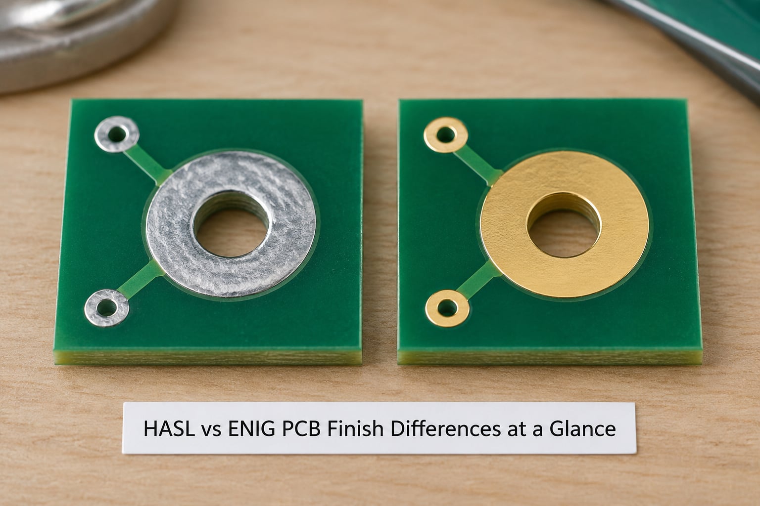
Here is the short version. HASL is measured in solder thickness and costs about 1x. ENIG is measured in nickel and gold thickness and lands roughly 1.8 to 2.5x the same board in ENIG. Everything else in the table is downstream of those two facts.
| Criterion | HASL (hot air solder leveling) | ENIG (electroless nickel immersion gold) |
|---|---|---|
| What sits on the pad | Molten tin-lead or tin-silver-copper solder | Electroless nickel-phosphorus with a thin immersion gold layer on top |
| Typical layer thickness | 1-3 µm of solder | 3-6 µm nickel plus 0.05-0.1 µm gold |
| Relative cost | 1.0x baseline | About 1.8-2.5x baseline |
| Surface planarity | Good, set by the air knife; varies pad to pad | Very good, closer to a photoresist surface |
| Fine-pitch suitability | Below 0.5 mm pitch is where problems start | Comfortable at 0.4 mm pitch and below |
| Solder joint behaviour | Solder wets solder; joints reflow and can be redone | Solder wets nickel through gold; joints form on the nickel surface |
| Shelf life, sealed and dry | About 6-12 months | One year and upward, often 3-5 years quoted |
| Oxidation and corrosion | Oxides on exposed copper and on the solder itself | Nickel is a diffusion barrier; gold does not oxidise |
| Rework by hand | Forgiving, the finish behaves like fresh solder | Possible but needs more heat, more flux, more care |
| Lead and RoHS | Leaded alloy is not RoHS; lead-free HASL is | Lead-free process |
| Known defect to manage | Uneven solder on fine pads, bridging risk | Black pad on the nickel-phosphorus layer |
| Typical applications | Prototypes, consumer electronics, industrial control, thick or through-hole boards | BGA and QFN land patterns, HDI, RF and telecom, medical, aerospace, long-storage builds |
What Is HASL PCB Finish?
HASL is a solder finish. The board is masked, then dipped into a pot of molten solder, then a jet of hot air blasts the excess off so the surface comes out level and flush with the copper. Hot air solder leveling is the oldest mainstream PCB finish still in daily production, and it is cheap because every step is a bulk chemical or thermal operation rather than a controlled deposition.
The process runs in three steps:
- Surface preparation. The board goes through a horizontal conveyor, gets degreased, micro-etched in acid, rinsed, and dried. This strips the oxide so the solder will actually grab the copper.
- Solder immersion. The board passes through a wave or a stencil-sprayed solder pot at around 260 °C and comes out coated in a film of molten alloy. At this temperature the solder wets the copper and dissolves a thin layer of it, which is what creates a real metallurgical bond rather than a mechanical smear.
- Air knife leveling. A vertical curtain of hot air shears off the solder above and below the pad. The pad ends up flat with the solder mask, typically 1-3 µm of solder remaining.
Leaded HASL uses a 63/37 tin-lead eutectic that melts at 183 °C. Lead-free HASL uses SAC305 (96.5% tin, 3% silver, 0.5% copper) that melts around 217-220 °C. That is a 35 °C or more jump in reflow temperature, and it is not cosmetic: the board spends longer at temperature, the laminate sees more thermal stress, and components with lower temperature ratings get less margin. RoHS restricted lead in 2006, so most new work is lead-free HASL unless someone specifically asks for the alloy.
What HASL is genuinely good at: wetting. Solder meeting solder forms a joint the way it was designed to, with no barrier layer in the way. It also means the pad can be reworked repeatedly, because you are literally adding heat to solder.
What Is ENIG PCB Finish?
ENIG is a plating stack, not a solder finish. Electroless nickel immersion gold puts a nickel-phosphorus diffusion barrier over the copper and then seals it with a very thin immersion gold layer. The nickel does two jobs: it stops copper diffusing upward into the solder, and it gives you a surface that does not oxidise before you get to it.
The process runs in four steps:
- Degrease, micro-etch, activate. Acid micro-etch removes the oxide; an activating bath cleans the last film off the copper so the next step can nucleate.
- Electroless nickel deposition. The board goes into an autocatalytic nickel bath. No current is applied because the reaction is chemically self-starting on the activated copper, which is how you get an even 3-6 µm on through-holes and blind vias that electroplating would miss.
- Immersion gold. A single dip into a gold solution. Displacement chemistry swaps the surface nickel atoms for gold atoms, so the gold layer self-limits at roughly 0.05-0.1 µm. It is a film, not a bath, which is why the gold figure looks so small.
- Rinse and dry. The board comes out with a uniform, matte, yellow-gold surface that resists handling marks and corrosion.
The gold is nearly pointless on its own. It exists to keep the nickel from oxidising and to survive handling and solder pot immersion without discoloring. The nickel layer is what your solder actually lands on.
One more ENIG variant worth knowing: ENEPIG adds a thin electroless palladium layer between nickel and gold. Palladium improves solderability, costs a little more, and is the usual answer when you need fine-pitch and worry about black pad.
Surface Appearance and Composition
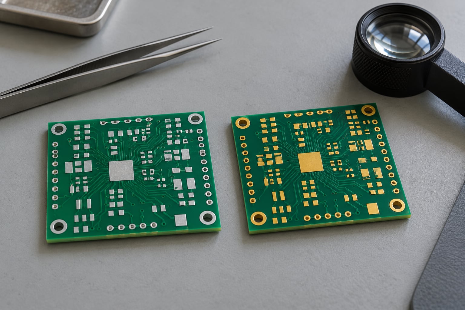
HASL pads look dull silver and slightly wavy under raking light. ENIG pads look matte yellow, uniform, and almost featureless. That visual difference is the most immediate clue to what you are holding, and assemblers pick it up on the board in seconds.
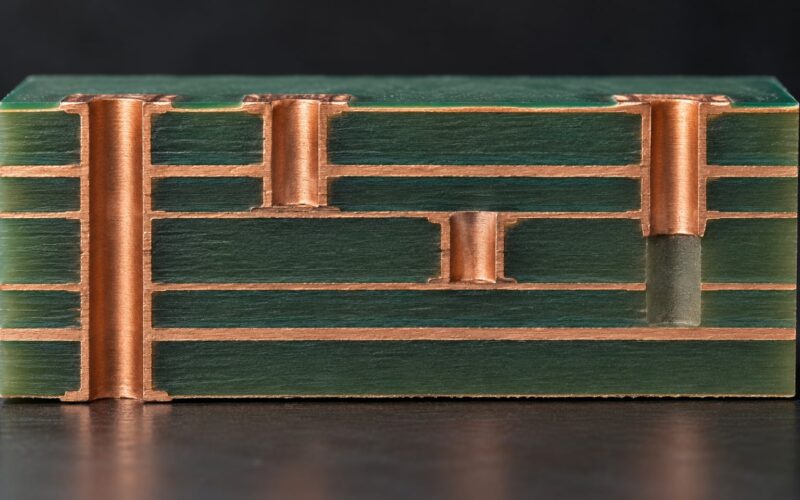
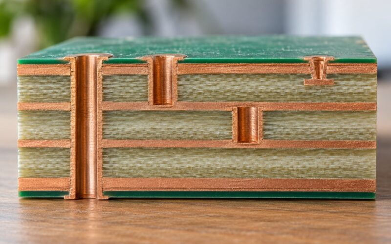
The layer stacks differ completely. HASL is one metallurgical layer of solder on copper. ENIG is three: copper, nickel-phosphorus, gold. That difference matters when you cross-section a joint. In ENIG, the intermetallic compound forms at the solder-to-nickel interface, which is slower than the copper-tin intermetallics in HASL. It is still a sound joint, it just forms on different physics.
Oxidation behaviour is where the gap widens. HASL solder is a tin alloy, and tin oxidises. Left unsealed in humid air it grows a tin oxide skin that solder will not wet, which is why bare HASL boards have a real shelf life limit. ENIG does not oxidise at all under ordinary storage, and the nickel blocks copper migration, which is a separate failure mechanism on long-dated boards.
For inspection, ENIG is easier to read under a microscope because everything is uniform. HASL needs a cross-section or a probe test to confirm the true solder thickness.
Solderability and Assembly Performance
HASL wets like solder to solder. That gives excellent wetting out of the box, but it also means the only thing keeping solder and copper apart during storage is the oxide that forms, and that is exactly what a good flux has to remove at reflow.
ENIG starts with clean nickel covered in gold, and gold dissolves into the solder almost instantly during reflow. That fast initial wetting is what makes ENIG hold up in demanding applications. The cost is a slightly slower intermetallic growth at the nickel interface than you get on copper.
A few practical assembly notes. With ENIG, solder paste prints and releases cleanly because the pads are flat and non-tacky; HASL pads that have been stored a while can hold paste poorly because of oxidation. In wave and reflow pots, ENIG boards pick up a small amount of dissolved gold into the solder pot, which can raise dross rates slightly over a long production run. HASL boards shed their own surface solder into the pot continuously, which some fabs prefer because the pot stays closer to alloy equilibrium.
Hand soldering is where the difference is most obvious, and it is the reason the exact question “ENIG or HASL for a prototype with small pitch and expectation to need rework” keeps showing up on engineering forums. On HASL you push a hot iron into an existing solder layer and it flows immediately. On ENIG you are heating nickel through gold, so you need more temperature, more dwell, and good flux. It works. It is just not forgiving, which is a real cost when the board is your only one.
Flatness, Planarity, and Fine-Pitch Designs
Flatness is the strongest technical argument for ENIG, and it is the one that decides most designs. An air knife shears solder off by force, so the finished pad height depends on how close the pad sits to the knife and how the solder wicks into the mask. On a wide-pitch board the variation is invisible. At 0.4 mm pitch with 0.5 mm pads on a QFN, that same variation is comparable to the gap between adjacent pads, and you get bridging or cold joints.
ENIG has no air knife. Thickness is set by bath time and chemistry, not by a jet, so pad-to-pad variation drops to a small fraction of the HASL spread. In practice, HASL becomes uncomfortable below about 0.5 mm pitch, and ENIG stays comfortable well below that. For 0.4 mm BGA, fine-pitch QFN, or any HDI design with buried vias, ENIG or ENEPIG is the default and HASL is the compromise.
Black pad: ENIG’s real weak spot
Black pad is a defect in the nickel-phosphorus layer, not in the gold. If the phosphorus content of the bath drifts low, or an immersion cycle runs long, the nickel surface can form a brittle phosphorus-rich layer with poor solder adhesion. The joint looks soldered, passes continuity, and then fails later as the plating delaminates.
Detection is straightforward: microsection a pad from an incoming lot and look for the interface between the solder and the nickel. Ask your fab for cross-sections as part of your first-article approval, and ask specifically what phosphorus content range their nickel bath runs and what their immersion gold time is. A fab that answers both questions precisely is a fab that controls the chemistry. The risk on any given board is low; the risk of choosing an uncontrolled shop is not.
HASL has no black pad. It has unevenness instead, which is annoying but visible and reliable.
HASL vs ENIG PCB Finish Cost
Nobody wins on price, and the honest way to say it is in multiples rather than per-board figures, which move with size, layer count and region. Take HASL as 1.0x and ENIG typically lands between 1.8x and 2.5x for the same board. For context, OSP sits a little above baseline and immersion silver in between.
The premium comes from three places. ENIG is a multi-step chemical process with several immersion baths and rinses, which is bath time and chemistry management rather than bulk thermal processing. The nickel bath is the expensive one, holding metals in solution at controlled temperature. And gold has a commodity price that moves, even at the thin weights involved, because the chemistry needs real gold purity to plate properly.
Where the premium stops mattering: high-density boards where bridging scrap rate exceeds the finish delta, boards bought once and stored for years, and anything with a wire bond or a fine-pitch land. Where it matters most: large double-sided boards at low volume, where a per-square-metre delta is a large share of the total. Prototypes feel it worst because the fixed setup charges get spread over a handful of panels.
Corrosion, Chemical Resistance, and Storage
Conflicting shelf-life figures are the most common complaint about this topic, and the reason is that sources quote different storage conditions. Under vacuum-sealed, desiccant-packed, humidity-controlled storage, lead-free HASL is commonly quoted at 6-12 months and ENIG at a year or more, with ENIG often listed at 3-5 years. Those numbers assume the packaging is intact.
In ordinary room air with the boards in an open anti-static bag, treat the lower end of those ranges as the real number. Humidity is what moves tin oxidation and what drives dendrite growth between closely spaced ENIG pads under a bias. Ask for your boards in sealed moisture-barrier bags with desiccant, and treat the surface finish as a shelf-life asset that the packaging protects.
Chemical resistance follows from the stack. Nickel is a passivating metal and handles most cleaning chemistry and flux residues well; gold on top resists tarnishing entirely. HASL has no barrier, so aggressive aqueous cleaning and long humid storage both work against it.
Which HASL or ENIG Finish Is Best for Common Uses?
Match the finish to the board rather than to the badge. My mapping, based on what actually drives the requirement:
| Application | Recommended finish | Why |
|---|---|---|
| Prototype, hand assembly, likely rework | HASL | Cheapest path to a board you can solder and resolder freely |
| Prototype with 0.4 mm pitch parts | ENIG or ENEPIG | Fine-pitch planarity outweighs cost at prototype stage |
| Consumer electronics, high volume | HASL | Cost per board dominates at volume with coarse pitch |
| Industrial control and instrumentation | Either | Choose on pitch and storage time, not environment |
| Automotive | ENIG | Long field life plus stored-inventory time before assembly |
| RF and high-frequency | ENIG | Uniform surface and no dendritic risk on fine features |
| Medical and diagnostic equipment | ENIG | Long shelf life and process traceability expectations |
| Aerospace, military, space | ENIG | Specified almost by default; also suits aluminium wire bonding |
| HDI, high-density interconnect | ENIG or ENEPIG | Blind vias and dense pads need uniform thickness |
| Boards stored longer than a year | ENIG | Oxidation resistance is the whole point |
Where OSP, immersion silver, and ENEPIG fit
OSP is an organic coating that costs barely more than HASL and gives a flat, uniform, lead-free surface. It is a good fit for fine-pitch lead-free work where you will not store the board long. Immersion silver is flatter still and cheap, but it tarnishes in sulfur-bearing air and is vulnerable to ionic contamination, so it needs good cleanliness and it is not for long storage. ENEPIG is the middle path between OSP cost and ENIG robustness. None of them replaces the other; they occupy different corners of the same cost-versus-stability grid.
HASL vs ENIG: How to Choose
Work through these six inputs and the answer usually falls out on its own:
- Smallest pitch. Below 0.5 mm, pick ENIG or ENEPIG. Above 1 mm, HASL is fine.
- Assembly process. Hand solder and rework expected means HASL. Automated reflow with a controlled profile works with either.
- Storage time before assembly. Under six months, either. Beyond a year, ENIG.
- Rework expectation. If you will pull and resolder parts, HASL is gentler on the board.
- Environment. Humid, corrosive, or safety-critical service argues for ENIG. Indoor consumer gear does not care.
- Volume. At volume, a few percent per board is real money. At prototype quantities, the absolute difference is often smaller than the setup charges you pay anyway.
When you write the order, be specific in the fab notes: name the finish, the alloy if it is HASL, the gold thickness and nickel phosphorus range if it is ENIG, the packaging you want, and your expectation on cross-section samples. Then ask your assembler what they prefer to receive, because an assembler who has to fix your joints absorbs your choice in their yield numbers.
Frequently Asked Questions
Is ENIG always better than HASL for a PCB?
No. ENIG wins on flatness, fine-pitch capability, shelf life, and corrosion resistance, and it usually costs about 1.8 to 2.5x the same board in HASL. HASL wins on cost, hand-soldering and rework ease, and thermal mass during assembly. For coarse-pitch boards that will be assembled soon, HASL is the better engineering choice. For anything below 0.5 mm pitch or stored more than a year, ENIG is the better one.
What is the main difference between HASL and ENIG?
HASL leaves molten solder on the copper pads and blasts the excess flat with hot air. ENIG deposits a 3-6 µm nickel-phosphorus layer by chemical reaction, then seals it with 0.05-0.1 µm of immersion gold. That is why HASL reflows like solder and is easy to rework, while ENIG gives a flatter, non-oxidizing surface that holds fine-pitch pads but needs more heat by hand.
Is HASL suitable for lead-free assembly?
Yes, and it is the default for most new work since RoHS restrictions. Lead-free HASL uses SAC305 solder, which melts around 217-220 °C against 183 °C for tin-lead. That 35 °C gap means longer time at temperature, more thermal stress on the laminate, and less margin for components with lower temperature ratings. Check your part ratings before committing to a lead-free reflow profile.
Which finish is better for fine-pitch components?
ENIG, or ENEPIG if your fabricator offers it. Air-knife leveling on HASL leaves pad-to-pad solder height variation that becomes comparable to the gap between pads below about 0.5 mm pitch, which is where bridging and cold joints show up. ENIG thickness is set by bath chemistry rather than by a jet, so planarity stays tight at 0.4 mm pitch and below. On coarser pitches the difference stops mattering.
Why is ENIG more expensive than HASL?
Three reasons. ENIG is a multi-bath chemical process rather than a bulk solder dip, which means bath time and chemistry control instead of a thermal operation. The electroless nickel bath is the expensive step. And real gold, even at the very thin weights used, carries a commodity price the fabricator passes through. The result is roughly 1.8 to 2.5x the cost of the same board in HASL.
Can a PCB with HASL be soldered more than once?
Yes, and that is one of HASL’s practical advantages. Because the pad is already solder, an iron or hot plate reheats the existing layer and the joint flows again, which makes part replacement and bodge wires straightforward. ENIG boards can also be reworked, but you are heating through nickel and gold, so you need higher temperature, more dwell time, and good flux. Expect more effort on your second and third passes.
Conclusion
HASL vs ENIG PCB finish differences reduce to one question: does your smallest pad force you to care about planarity? If yes, pay the 1.8 to 2.5x and take ENIG, ideally ENEPIG if black pad worries you. If no, and the board will be assembled within a year, HASL gives you better solderability and cheaper rework, and nobody will thank you for overpaying.
Before you send the order, resolve one thing: write down your minimum pitch and your maximum storage time, then check them against the table above. Everything else — alloy, gold weight, packaging, cross-section samples — is a detail you can add to the fab notes once those two numbers are settled.