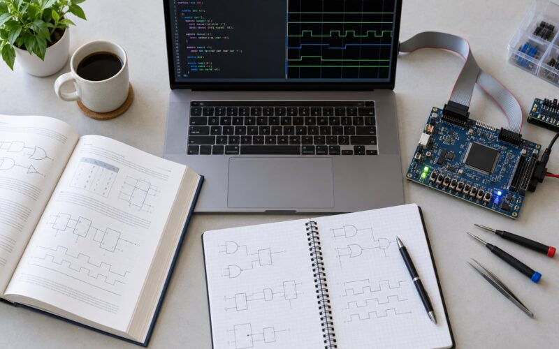
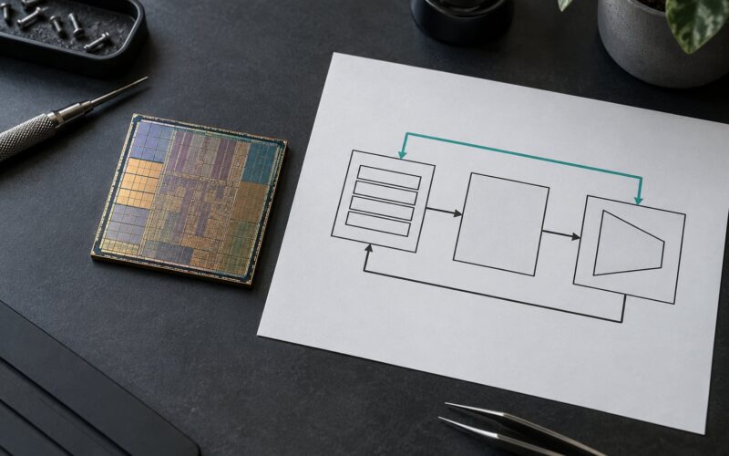
If you are an ECE or EE student aiming at a chip design role in 2026, the skills that matter most are synthesizable RTL in Verilog or SystemVerilog, a verification method such as UVM, timing analysis, physical design, and the DFT and low-power work that sits between them. Hiring managers screen for these because a chip cannot ship without every stage of the flow, and each stage has its own owner.
VLSI design is the process of building integrated circuits that combine very large numbers of components onto one die: system architecture, RTL coding, verification, logic synthesis, physical implementation, test, and signoff. The field feels enormous because it is genuinely broad, not because any single skill in it is exotic.
Here is the practical part. Each skill below is paired with where it is used, the job titles that depend on it, and one exercise you can complete to prove it. Most of these proofs come from free or open tools, so you do not need a commercial EDA license to start.
Table of Contents
- Skills to Learn for VLSI Design Jobs at a Glance
- 1. Digital Design and RTL Coding
- 2. Verilog, SystemVerilog, and Assertion-Based Design
- 3. Verification and UVM-Style Testbenches
- 4. CMOS Logic and Microelectronics Fundamentals
- 5. Digital Synthesis and Design for Manufacturability
- 6. Static Timing Analysis and Timing Closure
- 7. Physical Design and Place-and-Route Flows
- 8. Low-Power Design Techniques
- 9. Memory and Semiconductor Interfaces
- 10. SoC Architecture and System-Level Design
- 11. DFT, ATPG, and Design for Testability
- 12. EDA Tools, Scripting, Debugging, and Technical Communication
- Frequently Asked Questions
- What are the most important skills to learn for VLSI design jobs?
- Do I need to master every EDA tool before applying for an entry-level VLSI role?
- Is SystemVerilog or UVM more important for beginners?
- How can I build a VLSI design portfolio without commercial EDA tools?
- Which VLSI skills matter most for design verification roles?
- Should I learn front-end design or physical design first?
- Conclusion: Start With One Complete VLSI Design Flow
Skills to Learn for VLSI Design Jobs at a Glance
The table below is the shortest useful map of the field: one row per skill, with the flow stage it belongs to, the roles that need it daily, and the artifact that convinces a hiring manager you can actually do the work.
| Skill | Where it is used | Common job titles | Strongest proof of ability |
|---|---|---|---|
| Digital design and RTL coding | Front-end design, all blocks | RTL design engineer, design engineer II | A parameterized, verified block with a written specification |
| Verilog, SystemVerilog, assertions | Design and check authoring | RTL design, DV engineer | SystemVerilog testbench with coverage and assertion checks |
| UVM-style verification | Reusable, constrained-random environments | Design verification engineer | A UVM environment for a FIFO or protocol interface with closure evidence |
| CMOS and device fundamentals | Reasoning about speed, power, area | RTL, physical design, analog | An inverter-chain delay and power analysis you can explain |
| Synthesis and DFT awareness | RTL to gates, area and timing tradeoff | RTL design, synthesis engineer | Synthesis report with before-and-after area and critical path notes |
| Static timing analysis | Signoff timing closure | Physical design, STA, signoff | A fixed setup violation with the ECO you used and the slack recovered |
| Place and route flow | Floorplan, CTS, routing, extraction | Physical design engineer | A routed block with congestion and DRC-clean summary |
| Low-power design | Power intent and power-aware RTL | Low-power design, front-end, PD | A before-and-after dynamic power number from clock gating |
| Memory and interfaces | SoC integration, data movement | SoC integration, protocol engineer | A working AXI-Stream or AXI-Lite slave with handshake handling |
| SoC architecture | Partitioning hardware and software | SoC architect, subsystem lead | A small SoC with a DMA-driven accelerator and an address map |
| DFT, ATPG, MBIST | Test insertion and test economics | DFT engineer, design-for-test | A scan wrapper showing shift and capture, plus a memory test |
| EDA scripting, debugging, communication | Every stage, plus review | All design roles, EDA application engineer | A reproducible flow script and one well-written bug report |
One habit worth naming early: the strongest portfolios are built by going deep on two or three of these rows rather than skimming all twelve. Breadth matters for interviews, depth is what you get hired on.
1. Digital Design and RTL Coding
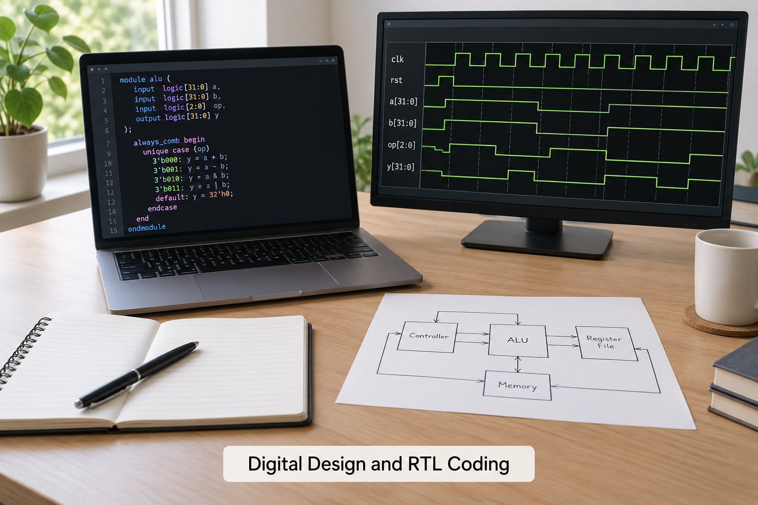
RTL coding is the core skill of front-end design, and it starts as plain digital design: combinational logic, flip-flops, counters, state machines, and the timing rules that govern them. If your combinational or sequential fundamentals are shaky, no amount of SystemVerilog fluency will rescue you in an interview.
The shift from textbook logic to real RTL is synthesis awareness. Anything you write must map cleanly to gates. Blocking assignments inside combinational always blocks create latches, inferred latches break timing closure, and clock gating written as an ordinary register just becomes an ordinary register.
Reset and clocking conventions are where interviews go wrong most often. Know the difference between synchronous and asynchronous reset, understand why a reset synchronizer exists for a released asynchronous reset, and know that a gated clock is a chip-stability problem, not a coding convenience.
For proof, build one small parameterized block: a counter or FIFO with a parameterized width and depth, plus a specification page stating the interface, latency, and edge cases. Write a testbench that proves the parameters actually work by instantiating more than one size. That single project exercises coding style, parameterization, reset handling and verification at the same time.
2. Verilog, SystemVerilog, and Assertion-Based Design
Verilog is the language everyone starts with, and SystemVerilog is the language most jobs require. SystemVerilog adds the object-oriented features that make large testbenches survivable: classes, inheritance, interfaces, packages, and constrained randomization.
The practical sequence is straightforward. Learn Verilog well enough to write synthesizable RTL and a self-checking testbench, then move to SystemVerilog for verification work and for cleaner RTL packaging. VHDL still appears in defense, FPGA, and European design houses, but Verilog and SystemVerilog dominate commercial digital design.
Assertions are the underrated half of the language. A concurrent assertion states a property the design must always satisfy, such as a valid signal never dropping before ready or a FIFO never overflowing. Assertions catch bugs that random stimulus can miss, because they check every cycle instead of sampling a few.
Here is a concrete example. For an AXI-Stream data path, assert that tvalid is never deasserted before tready, that tdata holds stable while tvalid is high and tready is low, and that tlast arrives exactly on the final beat. Those three properties cover most real AXI-Stream protocol bugs. Coding them as SVA properties makes the check permanent instead of a one-off debug step.
3. Verification and UVM-Style Testbenches
Verification is where the largest number of VLSI jobs sit, and it is the discipline most newcomers underestimate. Writing RTL that compiles is easy. Proving it never misbehaves across millions of cycles is the actual job.
Start with directed testing: a testbench you drive by hand through specific scenarios. That teaches you stimulus and checking. Then move to constrained randomization, where you let the simulator pick stimulus within declared constraints and hunt for rare corner cases you would never write by hand.
UVM, the Universal Verification Methodology, structures a testbench into reusable components: driver, monitor, agent, sequencer, scoreboard, and environment, connected through a phase mechanism and a factory pattern. You do not need to memorize the class hierarchy for an interview, but you should be able to explain what each component does and why the separation exists.
Functional coverage closes the loop. You define coverage groups and bins over states, transitions, and data values, then run until coverage converges and every bin has been hit. Coverage numbers are what a verification lead asks for at signoff, so learn to report them honestly, including what you excluded and why.
For proof, build a UVM environment for a small synchronous FIFO or a simple register interface. Show stimulus control, a scoreboard with a reference model, an assertion layer, and a coverage summary that reaches 100 percent on your defined bins. That artifact reads as engineering, not as coursework.
4. CMOS Logic and Microelectronics Fundamentals
CMOS knowledge is what lets you predict why a design is slow or hot instead of guessing. You need to know how a MOSFET switches, how an inverter consumes power through charging and leaking, and how delay scales with load capacitance and drive strength.
The core ideas are noise margins, propagation delay, dynamic power proportional to switching activity and capacitance, and the short-circuit current that flows during transitions. Learning the tradeoffs matters more than memorizing equations: a wider gate drives more current, improves delay, and burns more power.
Tie this to decisions you will actually make. Why does synthesis insert buffers? Why does a long wire cost more delay than a short one? Why does shrinking transistors reduce leakage power rather than raise it? These are the questions physical design engineers answer for a living.
A good exercise is an inverter-chain analysis. Build a chain of N inverters driving a capacitive load in ngspice, then sweep N and report delay and energy per transition. Then repeat with a NAND-based implementation. You will see sizing tradeoffs in a number rather than a diagram.
5. Digital Synthesis and Design for Manufacturability
Synthesis is the step where behavioral RTL becomes a gate-level netlist of standard cells. Knowing how it transforms your code is the difference between a design that hits its targets and one that leaves the back-end team a mess.
Read the synthesis report. Look at the critical path, the area breakdown, the number of flip-flops, and which logic got restructured. If area is far larger than expected, usually the cause is a wide comparator, a priority encoder, or a reset that was written as data.
Timing and area optimization is a negotiation. You can restructure an adder into a carry-select, share logic between states, or pipeline a path to trade area for frequency. You can also declare don’t-care conditions, which lets the optimizer pick the cheaper implementation, though careless don’t-cares create simulation and synthesis mismatches that are painful to debug.
Design for manufacturability starts here too. Rules about fanout limits, logic depth, and drive strengths decided in RTL save enormous back-end rework later. A design that synthesizes to a 200-cell-deep combinational cone is a design your physical design engineer will not thank you for.
For proof, synthesize a small ALU or counter with Yosys, publish the cell count and longest path, then change one line of RTL and publish the new numbers. A two-commit before-and-after in your repository tells a reviewer you understand the tool, not just the syntax.
6. Static Timing Analysis and Timing Closure
Static timing analysis checks every path in a design against clock requirements without simulating anything. Setup checks ask whether data arrives before the clock edge; hold checks ask whether it stays long enough after. Both must pass, and they are checked with uncertainty added to models that are already pessimistic.
Learn to read a report. Find the worst slack, trace the path from startpoint to endpoint, and identify whether the culprit is logic depth, fanout, a long net, or a badly placed register. Then look at clock domain crossings, where an asynchronous path needs a synchronizer and is timed as a false path or multicycle path.
The difference between analysis and engineering is the fix. A candidate who says a path fails is describing a report. A candidate who buffers a high-fanout net, moves a register back a stage, or up sizes a driver and then shows the recovered slack is doing timing closure.
Take a deliberately slow combinational block, run OpenTimer or any available timing engine on it, and record the failing path. Apply one ECO. Re-run, record the new slack, and explain in writing why the fix works and what it cost in area. Engineers respect a documented failed-then-fixed path far more than a clean report.
7. Physical Design and Place-and-Route Flows
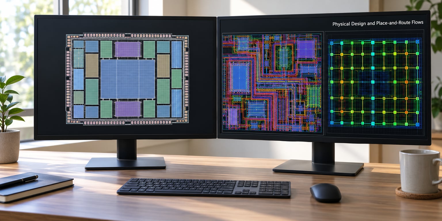
Physical design turns a netlist into a layout that meets timing, power, area, and manufacturability targets. The flow runs floorplan, then placement, then clock-tree synthesis, then routing, with power planning running alongside from the start and parasitic extraction feeding back into timing.
Each stage has a failure mode worth understanding. A bad floorplan makes everything downstream worse because wirelength and congestion follow the macro and memory placement. Poor CTS skews the clock and eats your setup margin. Routing congestion means the design does not fit its own channels, and fixing it usually means changing the floorplan, not pushing harder.
Power planning decides where power stripes go and how big the grid must be to carry current without unacceptable IR drop. Skew, congestion, DRC and LVS errors all come back to physical decisions made early, which is why a logical change can wreck a physical result even when it looks like a harmless one-line edit.
Proof here is visual and cheap. Run a small design through OpenROAD, publish a screenshot of the final layout with cell density, target density, routing congestion and DRC status, and write a paragraph on what you changed and why. If you have access to a commercial flow, quote Innovus or IC Compiler II in your resume only when you have genuinely used it.
8. Low-Power Design Techniques
Power is a first-class constraint now, not a cleanup step. Total power splits into dynamic power from switching activity and leakage power from idle transistors. At advanced nodes, leakage dominates when a block is inactive, which is why both halves need attention.
Clock gating stops toggling a clock when a register bank holds valid data, usually the single biggest dynamic power lever in a synchronous design. Power gating switches off an entire voltage domain, which is more aggressive and harder to verify because state can be lost. Multi-voltage domains let slow, low-leakage blocks run at a lower supply.
Designers express intent in UPF power specifications, and tools insert the structures during implementation. High-level synthesis can apply power optimizations earlier, and power-aware RTL means writing enable logic and data stability rules that a tool can exploit safely.
Verification is the part people miss. Any gated clock or powered-down domain needs an assertion that output is stable while the clock is off, or you will debug corruption in simulation for weeks. Measure before and after: run a switching-activity report, add gating to one block, and publish both power numbers with the area cost.
9. Memory and Semiconductor Interfaces
Most real SoCs spend their bandwidth moving data, so interfaces decide system performance. Know that SRAM is not DRAM: SRAM is fast, dense in logic, and volatile with no refresh, and it is what register files, caches and FIFO buffers are built from. Memory compilers generate the arrays and the surrounding periphery for a given process node.
On the protocol side, understand handshakes before you learn any specific bus. Valid and ready must not both be assumed to arrive together, back-pressure must be handled, and a stalled transfer must not lose or duplicate data. Once that is automatic, AXI-Stream becomes straightforward, and AXI with its five-channel read and write structure follows the same logic at a larger scale.
Know the rest of the picture too: DDR for external memory, PCIe for high-speed serial links, and USB and Ethernet for peripherals and networking. You will not implement SerDes PHY design in a fresher role, but interviewers ask what each is for and what the bandwidth and protocol overhead tradeoffs are.
For proof, write an AXI-Stream slave that handles back-pressure and packet boundaries, then test it with a source that randomly stalls. A testbench that only ever drives ready-high has verified nothing, which is exactly what an interviewer will ask you about.
10. SoC Architecture and System-Level Design
System-level design is deciding what goes in hardware, what stays in software, and how the pieces talk. The core objects are CPU subsystems, memory controllers and caches, DMA engines, accelerators, interrupt controllers, and the interconnect that connects them.
The address map is where architecture becomes concrete. Every peripheral occupies a range, and every range has an access type: memory-mapped registers, read-only configuration, or coherency rules for caches. Interrupt design decides whether your system is responsive or thrashes, and DMA decides whether the CPU wastes cycles copying buffers instead of computing.
A hardware-software partition is a real trade. Put filtering in hardware and you gain throughput and lose programmability. Put it in firmware and you keep flexibility and lose power and latency budget. Good architects make that call deliberately and write down why.
For proof, take a small processor core and add a DMA-controlled accelerator with its own registers, an interrupt line, and a documented address map. Show the register interface in your write-up. Hiring managers look for whether you can describe interfaces and ownership boundaries, not whether the block wins a benchmark.
11. DFT, ATPG, and Design for Testability
A chip that works on the tester but has a manufacturing defect costs far more than the design effort saved by skipping test. Design for test inserts structures that make defects findable, and DFT engineers own that structure.
Scan chains convert sequential elements into a shiftable path so an external tester can load a pattern, capture a response, and compare it. Scan costs area, adds routing, and slows the clock slightly, so the designer and DFT engineer negotiate insertion to keep coverage high without wrecking timing. Boundary scan, usually accessed through JTAG, is the access mechanism that makes all of this reachable.
ATPG is the pattern generation: given the netlist and an internal node, the tool finds a pattern that excites a stuck-at fault and propagates it to an observable output. Stuck-at coverage is the standard metric. MBIST handles memories separately, since regular scan cannot practically test every memory bit, by running a built-in test algorithm on-chip and reporting pass or fail.
For proof, wrap a small block in a scan shell and show the shift, capture, and compare sequence in a waveform. Add a simple memory test next to it and explain why scan alone is not enough for the RAM. That contrast is the whole interview question in one screenshot.
12. EDA Tools, Scripting, Debugging, and Technical Communication
Nobody hires you for the GUI. They hire you for flow ownership: reading a specification, owning a block, and driving it from RTL through signoff with the tools that stage requires, whether that is Synopsys, Cadence, or Siemens EDA.
Scripting is what turns flow knowledge into an edge. Tcl is the native language of most EDA tools and lets you automate a synthesis or place-and-route run. Python is the default for data handling, report parsing, regression management and waveform analysis. Learn to run Linux well, use Git properly with meaningful commit messages, and write scripts that someone else can run without asking you questions.
Debugging is its own skill. Learn to read a log instead of scrolling it, learn to slice a waveform around the first failing cycle, and learn to bisect a regression. When something breaks, the fastest engineers narrow the search space before they start guessing.
Communication decides how far your work goes. Write design documents with interface tables, register maps, and assumptions stated explicitly. Write bug reports a stranger can reproduce: symptom, environment, steps, expected, observed. Review peers’ code, and take review feedback without ego. On a chip team your design will be read more often than it will be debugged.
For proof, publish one reproducible flow script and one bug report that someone else actually used. Include what went wrong in a project write-up, which is the part most portfolios omit and the part reviewers notice first.
Frequently Asked Questions
What are the most important skills to learn for VLSI design jobs?
The four that come up in almost every posting are synthesizable RTL in Verilog or SystemVerilog, verification with a real method such as UVM or assertions, timing analysis, and familiarity with the synthesis and place-and-route flow. Add DFT and low-power awareness and you cover most entry-level roles across RTL, verification, and physical design.
Do I need to master every EDA tool before applying for an entry-level VLSI role?
No. Employers care that you understand the stage the tool serves, not that you have clicked every menu in it. Learn one simulator, one synthesis tool, and one place-and-route or timing tool deeply enough to explain a report, then learn to read documentation for the rest. Tool names change faster than the underlying flow does.
Is SystemVerilog or UVM more important for beginners?
Learn Verilog first, then SystemVerilog, then UVM. SystemVerilog is the language you write both design and checks in, so it is the foundation. UVM is a class-based layer built on top of it, and it only clicks once you are comfortable with classes, interfaces, and constrained randomization in plain SystemVerilog.
How can I build a VLSI design portfolio without commercial EDA tools?
Use the open-source flow: Icarus Verilog or Verilator for simulation, Yosys for synthesis, OpenROAD for place and route and DRC, OpenTimer for timing, ngspice for analog SPICE, and OpenLane for an end-to-end RTL-to-GDSII run. Document the setup, the reports, and what broke. The engineering thinking transfers even when the tool names do not.
Which VLSI skills matter most for design verification roles?
SystemVerilog in depth, UVM component architecture, constrained randomization, functional coverage closure, assertion-based checking, and waveform debugging with a tool such as Verdi or a GUI debugger. Verification engineers are judged on bugs found and coverage reached, so every project write-up should state what your testbench would have caught.
Should I learn front-end design or physical design first?
Start with front-end RTL because it teaches you what you are building and gives you the fastest feedback loop. Physical design follows naturally once you understand timing, since STA is the constraint the whole flow optimizes. If you enjoy layout and floorplanning problems, moving to physical design after a year of RTL is a solid path.
Conclusion: Start With One Complete VLSI Design Flow
Pick one small block this week, write a one-page specification for it, and take it all the way through: RTL, a self-checking testbench, synthesis, timing analysis, and a written summary of what failed and why. One block taken end to end teaches more than a dozen tutorials half finished.
Then add the second block, push the first one into place and route, and start publishing the reports. In 2026, the engineers getting the strongest offers are the ones who can show a complete flow and explain every number in it.