A yield engineer job description centers on one job: raising the share of working chips that come off each wafer without spending years rebuilding the process to do it. These engineers read production data, find the defects eating output, prove where they come from, and work with process, design, and equipment teams until the losses stop coming back. It is the difference between watching a yield number and moving it.
Wages sit well above the average engineering role in most US fab hubs, and the work is increasingly data-heavy rather than purely hands-on. If you have been searching job boards for “yield engineer job description explained” and want to know what the posting actually asks you to do all day, here is the honest version.
Table of Contents
- Yield Engineer Job Description Explained
- What Does a Yield Engineer Do?
- Defect analysis and failure analysis
- Process monitoring and statistical control
- Wafer disposition
- Root cause analysis and experimentation
- Yield reporting and modeling
- Cross-functional work
- Which Semiconductor Yield Metrics Matter Most?
- What Is a Typical Yield Engineer Workflow?
- What Skills and Qualifications Does the Job Require?
- Commonly required
- Often preferred
- Yield Engineer Job Description Explained by Industry Sector
- Wafer foundries
- Integrated device manufacturers
- Fabless companies
- Equipment suppliers
- Advanced packaging and test
- What Does a Yield Engineer Job Description Typically Include?
- Responsibilities, copy-ready
- Typical qualifications, copy-ready
- How Much Does a Yield Engineer Earn?
- How Do You Become a Yield Engineer?
- Frequently Asked Questions
- Do you need an engineering degree to become a yield engineer?
- What software and tools do yield engineers use?
- Is a yield engineer the same as a process engineer?
- Do yield engineers work night shifts or travel?
- Which industries hire yield engineers?
- How can someone get semiconductor experience without a fab job?
- Conclusion
Yield Engineer Job Description Explained
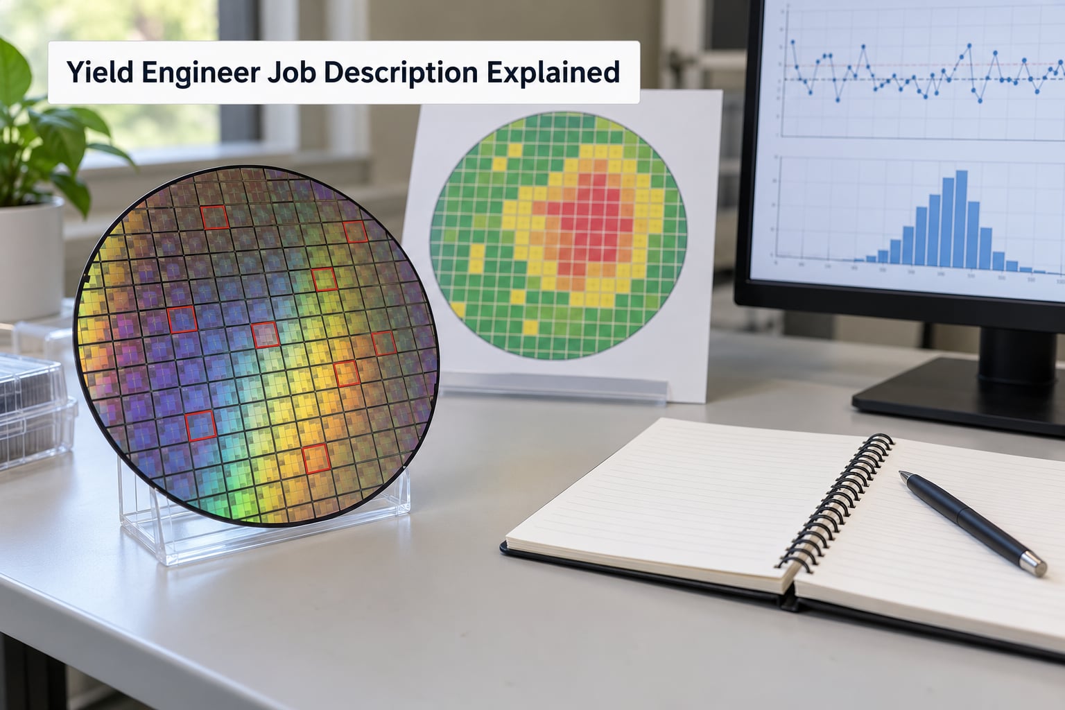
A yield engineer is a semiconductor manufacturing specialist who finds, ranks, and eliminates the loss mechanisms that keep good die from shipping. They study defect maps, inline measurements, electrical test results, and process tool history to work out which defect costs the most material, then close it with a process or design change that holds.
Yield is the link between how a chip is designed and what the factory actually produces. A design that performs perfectly on paper can still yield badly if one step in the fab leaves particles on the wafer or shifts a transistor threshold. The yield engineer sits between those two worlds.
That is what separates the role from general production or process engineering. Process engineers own the recipe and the equipment for a step. Production engineers own throughput and schedule. Yield engineering owns the outcome across the whole flow, and it is judged by a measurable number rather than a recipe that looks reasonable on paper.
What Does a Yield Engineer Do?
The scope is broader than most people expect. Posting lists describe the headline as “yield and failure analysis,” but the daily work runs across eight or nine connected activities.
Defect analysis and failure analysis
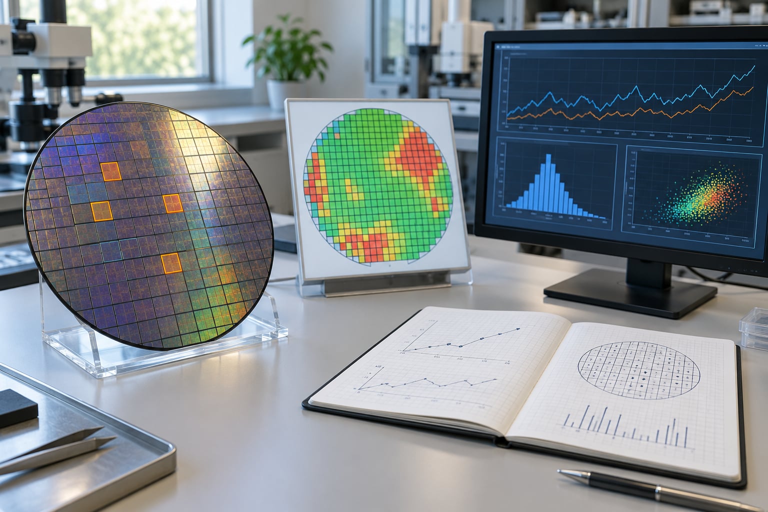
They review wafer maps and defect inspection output to see where defects cluster. A cluster at the wafer edge points to a handling or chuck problem. A radial pattern points somewhere else entirely. Then physical and electrical failure analysis narrows it down to a specific mechanism.
Process monitoring and statistical control
Inline metrology generates far more data than anyone can eyeball. Yield engineers track whether measurements sit inside control limits and whether the drift is statistically real before reacting.
Wafer disposition
When a lot looks bad, someone has to decide: ship it, rework it, sort it, or scrap it. Yield engineers hold that authority more often than candidates expect, because the call is economic as much as technical.
Root cause analysis and experimentation
Once a mechanism is suspected, they design a controlled experiment or split-lot trial to prove it. Guessing wastes wafers, and wafers are the most expensive thing in the building.
Yield reporting and modeling
They build yield models, forecast where a new product will land, and report loss distributions to the teams who plan capacity and cost. Forecasts built from historical excursion data are how a ramp gets planned rather than merely survived.
Cross-functional work
Most fixes are not owned by one group. A change to a deposition step might come out of an equipment engineer’s maintenance data and a process engineer’s recipe, and it will need design input too. Practitioners describe the collaboration as constant rather than occasional.
Which Semiconductor Yield Metrics Matter Most?
You will see these terms in every posting and every performance review. Learn the distinctions before your interview, because the difference between functional and parametric yield is a common question.
| Metric | What it tells you | How yield engineers use it |
|---|---|---|
| Die yield | The share of individual die on a wafer that pass all tests | The most direct measure of output; sets wafer cost per good chip |
| Wafer yield | Good die divided by total die across a wafer or a group of wafers | Baseline performance for a process and product |
| Lot yield | Yield across a batch of typically 25 wafers | How well the recipe and equipment held up over a production run |
| First-pass yield | Yield on the first attempt, before rework or salvage | The honest signal on whether the process is stable, since rework flatters the number |
| Parametric yield | Share of die meeting electrical specs but not fully passing functional test | Early warning: parameter drift shows up before hard failures do |
| Defect density | Defects per unit area, usually per square centimeter | Points at which process step or tool is adding particles |
| Process capability | How well measurements fit within specification limits | Separates real process shifts from ordinary noise |
Good yield engineers distrust a single number. A first-pass yield that looks healthy can still hide a defect mechanism that gets worse as the node shrinks, so they watch defect density and parametric yield beside the headline percentage.
What Is a Typical Yield Engineer Workflow?
Most weeks are spent inside an investigation loop rather than on a fixed schedule. The loop looks roughly like this.
- Review the data. Overnight lots come in with a yield below expectation. The engineer pulls the lot history, the wafer map, the defect breakdown, and the tool charts.
- Confirm the excursion is real. A test system problem can mimic a process problem, so the first step is often ruling out the measurement itself.
- Contain the material. Affected wafers get held, and neighboring process steps get checked before more material is exposed. Containment protects output while the root cause is still unknown.
- Find the mechanism. Cross-sectioning, electrical probing, correlation with tool and recipe history, and comparison against good wafers from the same period.
- Test the fix. A split-lot or designed experiment runs so the change is measured against a control, not admired in isolation.
- Watch the response. Yield moves over days, not minutes. Closing too early means coming back to the same excursion later.
- Close or reopen. The issue gets documented, the fix gets transferred to the standard recipe, and monitoring stays in place for a defined period. If yield drifts back, the issue reopens.
Ramp periods compress this loop. Practitioners describe production ramps as the hardest stretch of the job, with long hours and steady pressure to get a new product to spec.
What Skills and Qualifications Does the Job Require?
Postings split cleanly into required and preferred items, and the required list is shorter than candidates expect.
Commonly required
- A bachelor’s degree in electrical engineering, chemical engineering, materials science, mechanical engineering, or a related field
- Applied statistics: control charts, capability analysis, hypothesis testing, regression
- Working knowledge of wafer fabrication flow and what each major step contributes to yield
- Defect inspection and failure analysis techniques, including how to read a wafer map
- Scripting and data analysis, usually Python or SQL
- Clear written documentation, since findings have to survive contact with other teams
Often preferred
- Machine learning and data mining applied to large inspection datasets
- Statistical process control in a regulated or high-volume environment
- Experience supporting technology transfer or new product qualification
- Risk assessment and process change management practice
- Six Sigma Green Belt or Black Belt
The statistical side has grown the fastest. On advanced nodes, the signal-to-noise problem is hard enough that manual review of inspection output no longer keeps up, and several postings now list machine learning explicitly rather than as a nice-to-have.
One thing worth deciding early: how much you want to be inside the cleanroom. Failure analysis and physical cross-sectioning happen in person, and the role is not remotely deliverable in the way software work often is.
Yield Engineer Job Description Explained by Industry Sector
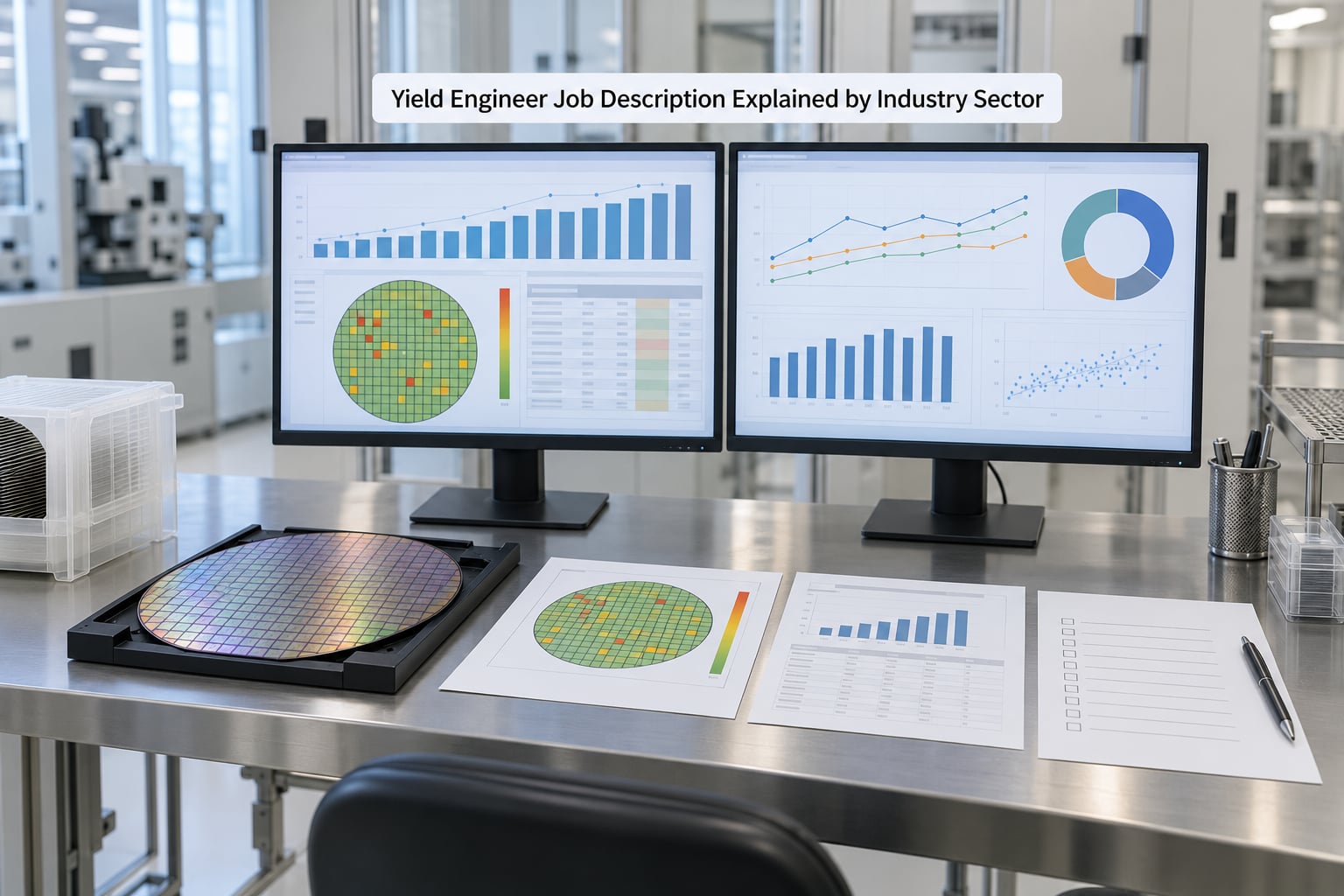
The title means slightly different things depending on who is hiring, and the same words appear in quite different job descriptions.
Wafer foundries
Foundry yield engineers own a process technology across many customers. The work leans on statistical control, defect reduction, and cross-node transfer, with less design coupling and a strong focus on consistency over long production runs.
Integrated device manufacturers
At an IDM the product is fixed and known, so yield engineers work closer to design and product engineering. Failure analysis on specific products, qualification support, and ramp readiness take up more of the description.
Fabless companies
With no factory of their own, these engineers monitor their foundry’s output, run correlation and program analysis on test data, and escalate to the supplier. Supplier management and data analysis replace hands-on process work.
Equipment suppliers
Here the job is defined by the tool. Installers and applications engineers feed field defect data back to engineering, which is closer to reliability and process integration than to fab yield ownership.
Advanced packaging and test
Packaging yield work concentrates on assembly, interconnects, and known-good-die handling rather than front-end wafer defects. Test engineering and statistical binning data play a bigger part.
Common to every setting: defect analysis, data-driven root cause work, and reporting that connects technical findings to shipped material.
What Does a Yield Engineer Job Description Typically Include?
Most real postings are built from a short, repeatable list. This is the pattern you will see most often, written so you can compare it against anything you are reading.
Responsibilities, copy-ready
- Perform yield and failure analysis to identify root causes of defect and parametric loss
- Monitor manufacturing data and flag process excursions against control limits
- Define and maintain wafer disposition rules with process and quality teams
- Design and run experiments that verify process changes before full adoption
- Transfer fixes into standard recipes and confirm the response holds over time
- Report yield performance, loss breakdown, and improvement plans to stakeholders
- Support technology transfer, new product qualification, and production ramps
- Apply statistical methods, data mining, and machine learning to large inspection datasets
- Partner with process, equipment, design, and product engineering on corrective actions
Typical qualifications, copy-ready
- Bachelor’s degree in electrical, chemical, materials, or mechanical engineering
- Solid grounding in statistics and statistical process control
- Familiarity with wafer fabrication and defect inspection methods
- Proficiency with data analysis tools; scripting ability is often required
- Clear communication across technical and non-technical audiences
Treat any single posting as one company’s needs, not the whole field. A foundry and a fabless company will both call the role “yield engineer” and want different things from you.
How Much Does a Yield Engineer Earn?
US pay for the role tracks experience closely and skews well above general engineering averages, with the biggest premiums in fab hubs. Treat these as typical ranges, not offers.
| Level | Typical US range (annual base) | What changes the number |
|---|---|---|
| Entry level, new graduate | roughly 70,000 to 95,000 | Degree strength, internship experience, location |
| Mid level, 3 to 7 years | roughly 100,000 to 140,000 | Node and technology ownership, ramp experience |
| Senior, 7 to 12 years | roughly 140,000 to 185,000 | Scope of products owned, people leadership |
| Staff, principal, or manager | roughly 175,000 to 240,000 and up | Organization-wide process ownership, equity structure |
One published process integration and yield engineer posting at a large US chipmaker listed a range of about 147,000 to 189,000 a year, which shows how much the upper bands move once a role carries ownership of a specific process.
Four factors move the number most: the company’s band structure, the location, the node or technology you own, and how specialized your skills are. Silicon carbide, gallium nitride, and advanced packaging work tend to pay above general logic roles. Current postings are the only accurate source, since pay bands shift with the labor market and never match a salary site exactly.
How Do You Become a Yield Engineer?
The honest challenge is that entry-level yield postings are rare. Most people get in sideways, and there are several reliable routes.
- Start in process engineering. The most common path. Own a step, learn what good control looks like, then move to the output.
- Take a manufacturing or quality role. Statistical process control and disposition experience transfers directly, and quality engineers often move into yield later.
- Work as a technician or equipment engineer. Hands-on time with tools and defect inspection is genuinely valued, and it builds the physical failure analysis instincts the role needs.
- Use internships. A summer in a fab, a process integration group, or a yield analysis team counts more on a resume than unrelated coursework.
- Build the data skills independently. Python, SQL, and statistics practice on public datasets demonstrates the analytical side before anyone hires you for it.
A useful signal for whether a role is a good fit: if you enjoy hunting for the one explanation behind a pile of numbers, this work rewards that. If you would rather build something than investigate why it failed, design or process integration may suit you better.
Frequently Asked Questions
Do you need an engineering degree to become a yield engineer?
Almost always, yes. The large majority of US postings ask for a bachelor’s in electrical, chemical, materials, or mechanical engineering. A few accept a statistics or physics degree paired with semiconductor coursework or a relevant technical role. Some fabs hire technicians and equipment engineers without a four-year degree, but those hires are usually for adjacent work rather than the engineer title itself.
What software and tools do yield engineers use?
The daily stack is data and analysis rather than one design package. Practitioners report using JMP, Python, and SQL as standard, pulling from manufacturing execution and defect inspection systems such as KLA systems, plus statistical process control software for charting and capability analysis. Exact platforms differ by company, so learn the concepts and be ready to learn a vendor system quickly.
Is a yield engineer the same as a process engineer?
No, and confusing them is the most common career mistake. Process engineers own the recipe and tool performance for a specific step. Yield engineers own the output across many steps, find what is costing the most good die, and close it. They overlap constantly and many people move between them, but the accountability is different: recipe ownership versus results ownership.
Do yield engineers work night shifts or travel?
Most do not work a fixed night shift, but the role follows the problem rather than the clock. A yield excursion at 2am will pull someone in, and ramp periods bring long weeks. Travel is usually limited to a few days at a time for equipment training, supplier visits, or site qualification, since the fab itself is a fixed location you report to.
Which industries hire yield engineers?
Wafer foundries, integrated device manufacturers, and memory makers are the core hirers, along with equipment suppliers and advanced packaging operations. Fabless chip companies also employ yield engineers to monitor foundry partners and analyze test data. Outside semiconductors, solar cell manufacturing and electronics assembly use similar defect and yield analysis methods under different job titles.
How can someone get semiconductor experience without a fab job?
Start where fab data is reachable. Open-source datasets and public failure analysis material teach defect patterns and wafer map reading. Personal projects that analyze inspection or test data in Python and SQL demonstrate the analytical side directly. University research cleanrooms, semiconductor bootcamps, and equipment supplier internship programs are the most reliable on-ramps to hands-on time.
Conclusion
A yield engineer job description comes down to measurable output: find the defect mechanism costing the most good die, prove it with data, close it with a change that holds, and document it so the same loss does not return. Everything else in the posting, from wafer disposition to machine learning on inspection data, supports that loop.
If you are aiming at the role, do three things now. Build real statistical fluency, since it separates candidates faster than any other skill. Practice reading a wafer map and a control chart until you can describe what is wrong without guessing. Then open a current semiconductor yield engineering posting and match your background to its required list line by line, because the details shift by company and technology. Roles in this field move as 2026 hiring cycles do, and current postings tell you far more than any general article.