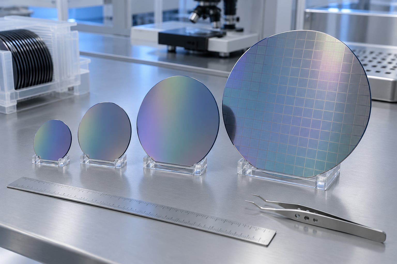
Wafer size evolution is a staircase, not a leap. Since the early 1980s the industry has climbed from roughly 100mm (4-inch) wafers through 125mm and 150mm (6-inch), on to 200mm (8-inch) in 1990, and finally to 300mm wafers that measure 11.81 inches and are called 12-inch in the trade. How wafer sizes evolved from 100mm to 300mm tracks one variable closely: usable area per wafer, which grows with the square of the diameter, so every step up spreads the same processing cost across more dies.
As of 2026, the 300mm wafer is the volume standard for leading-edge logic, DRAM and NAND, while 200mm capacity is tight and heavily in demand for analog, power and automotive parts. Smaller diameters are still made for specialty devices, compound semiconductors and research lines.
Table of Contents
- How Wafer Sizes Evolved from 100mm to 300mm
- How wafer sizes evolved from 100mm to 300mm in six steps
- 100mm to 150mm: The Era of Smaller Mainstream Wafers
- Why 100mm became the first volume standard
- Why 150mm replaced it, and why 100mm stayed
- 125mm as the compromise
- 200mm Wafers: The 150mm Successor Takes Hold
- 300mm Wafers: How the Industry Reached the 11.8-Inch Standard
- Why Did Wafer Sizes Increase?
- What Does Wafer Size Mean for Chip Output?
- How Did Larger Wafers Change Semiconductor Equipment?
- Did Moving from 100mm to 300mm Always Reduce Chip Costs?
- Are Smaller Wafers Still Used Today?
- What Comes After 300mm Wafers?
- Frequently Asked Questions
- Is a 300mm wafer the same as a 12-inch wafer?
- How many chips can fit on a 300mm wafer?
- Does a 300mm wafer mean the chips use a newer process node?
- Why did the semiconductor industry skip 175mm wafers?
- Why are 100mm and 150mm wafers still manufactured?
- Conclusion
How Wafer Sizes Evolved from 100mm to 300mm
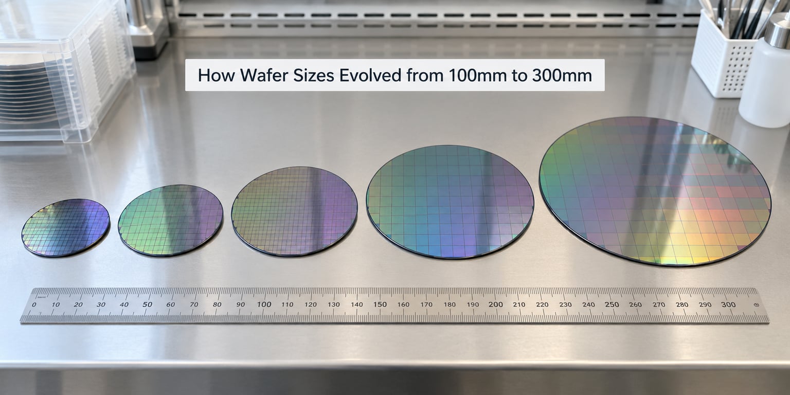
The four commercial standards that matter are 100mm (4 inch), 150mm (6 inch), 200mm (8 inch) and 300mm (11.81 inch, sold as 12 inch), with 125mm (5 inch) as a transitional size that skipped straight past 175mm. Each transition happened when device density grew enough that the fixed cost of running a process could no longer be spread over too few dies.
| Diameter | Inch equivalent | First volume production | Key driver | Gross area vs previous standard |
|---|---|---|---|---|
| 100mm | 3.94 in (called 4 in) | Early 1980s | Volume production of mature-node integrated circuits | Baseline |
| 125mm | 4.92 in (called 5 in) | Mid 1980s | Intermediate step for memory and analog parts | 1.56x |
| 150mm | 5.91 in (called 6 in) | Mid to late 1980s | Rising device density, analog and early memory | 2.25x |
| 200mm | 7.87 in (called 8 in) | 1990 | PC and telecom demand, cost per die | 1.78x |
| 300mm | 11.81 in (called 12 in) | Early 2000s, tipping point around 2012 | Leading-edge logic, DRAM, 3D NAND | 2.25x |
| 450mm | 17.72 in | Not in volume production | Studied by the G450C and F450C consortiums | 2.25x (theoretical) |
How wafer sizes evolved from 100mm to 300mm in six steps
- Before 100mm: 1 inch, 2 inch and 3 inch wafers. Diameter was set by what could be pulled as a single Czochralski boule and handled by hand-operated slicing and polishing equipment.
- 100mm, early 1980s: The first diameter large enough for real volume integrated-circuit production, with enough area for several large bipolar and early MOS dies per wafer.
- 125mm, mid 1980s: A deliberate intermediate step. Suppliers and fabs moved up without committing to a full 150mm tool set.
- 150mm, mid to late 1980s: Became the mainstream standard for analog, memory and microcontroller work, and stayed dominant into the mid 1990s.
- 200mm, from 1990: The first 200mm line combined IBM process technology with Siemens factory engineering. Adoption ran through the 1990s and 2000s and then went into decline at the leading edge.
- 300mm, from the early 2000s: The 2012 shift to 300mm produced more than 2.25 times as many dies per wafer, with roughly 96% adoption across leading-edge output at that point.
Note what is missing from that list. There was never a commercial 175mm standard, because the cost of running two tool sets in parallel is far worse than the cost of jumping straight from one standard to the next.
Before 100mm, the bottleneck was the crystal itself. A boule grown from the Czochralski process could only be pulled thick enough to survive slicing, lapping and polishing without cracking, and small-diameter ingots were far easier to handle. Once ingot growth, wire sawing and polishing matured, the constraint moved to the fab, and the fab could suddenly handle much wider wafers.
100mm to 150mm: The Era of Smaller Mainstream Wafers
Why 100mm became the first volume standard
100mm wafers carried the integrated circuit out of the hybrid and low-volume era. A die of a few square millimetres still fit dozens of times over on a 100mm wafer, which meant one pass through diffusion, lithography and metallisation produced a meaningful number of identical chips.
The devices of that period set the pattern that still holds. Bipolar analog, op-amps, regulators and early microcontrollers used large die area for relatively coarse functions, so their cost advantage scaled directly with wafer area. Fab utilisation mattered enormously: a partly empty 100mm wafer wasted most of the capital already sunk into the tool.
Why 150mm replaced it, and why 100mm stayed
When designers moved to denser logic and early memory, die area shrank faster than process costs rose. At that point more dies per wafer meant the same fixed cost divided further, and 150mm won the mainstream by a wide margin in the late 1980s.
100mm and 150mm coexisted far longer than people expect. Analog and power parts did not shrink much, their volumes were lower, and the existing 100mm tool set was already paid for. A fab running a mature 100mm process could hold good utilisation without buying new equipment, which is exactly the argument that keeps 200mm capacity busy today.
125mm as the compromise
125mm wafers served as a bridge for suppliers and fabs that wanted more area than 100mm offered but did not want to rebuild for 150mm. It also mattered for silicon wafer suppliers, who could sell more prime area per boule without moving their crystal-pulling equipment to a much larger diameter.
200mm Wafers: The 150mm Successor Takes Hold
The 200mm era started with a joint effort in 1990 combining IBM process technology and Siemens factory engineering for the first 200mm line. Roughly 70 200mm lines were operating by 1995, capacity peaked around 2007, contracted after the 2008 financial crisis, and by 2015 only about 178 lines remained.
Process generations moved with the format. The 200mm format carried much of the 0.5 and 0.35 micron generation, then the 0.25 and 0.18 micron generations, and it is still widely used at 90 and 130 nanometre nodes for analog, power management, automotive and industrial microcontrollers, image sensors and RF devices.
Getting there operationally was harder than the headline suggests. Spin coaters, stepper scanners, chemical mechanical planarisation tools, thermal process furnaces and inspection equipment all had to be rebuilt or requalified for the wider carrier. Load ports grew, FOUP handling became the default, robotic transfer had to hold flatness and bow and warp across a larger disc, and spin coat uniformity and anneal uniformity across the radius became harder to hold.
One historical footnote is worth knowing, because it shows the industry has tried intermediate sizes before. In the early 1970s ITT Semiconductors moved from 2 inch to 2.25 inch wafers with essentially one change: a larger chuck. That trick does not scale to a step of 100mm or more.
300mm Wafers: How the Industry Reached the 11.8-Inch Standard
A 300mm wafer measures 300 millimetres, or 11.81 inches, and is sold as a 12-inch wafer because fabs and equipment suppliers label it in whole inches. It is not 12 inches exactly, and the difference shows up in handling and load port design.
Intel, Toshiba, Samsung and TSMC were among the companies that pushed 300mm into volume production through the 2000s, and the format crossed from promising to default around 2012. That is the year the shift to 300mm delivered more than 2.25 times the dies per wafer of 200mm and reached roughly 96% adoption on leading-edge output.
Three things drove it. Leading-edge logic dies stopped shrinking in area as fast as feature sizes shrank, so the only way to hold cost per good die down was more die per wafer. Memory went the other way, stacking more layers into taller and denser DRAM and 3D NAND structures that put a large share of the wafer’s value into a single die. And capital cost per wafer of output fell far enough that a fab built around 300mm could undercut an equivalent 200mm fab on the same node.
Thickness moved in the opposite direction at the same time. A 300mm wafer is wider, so it can be made thinner without losing stiffness in handling, and wafer thinning became routine for stacked products. In October 2024 Infineon announced ultra-thin 300mm silicon wafers at roughly a quarter the thickness of a human hair.
Why Did Wafer Sizes Increase?
- More die per wafer. Area scales with the square of diameter, so the same die fits 2.25 times as often on 300mm as on 200mm.
- Capital and operating economics. Every lithography, etch, deposition, furnace and metrology tool amortises its cost across more output per cycle, which is the core of cost per die reduction.
- Electronics demand. Personal computers, telecom equipment, memory and now data centre accelerators all consume enough silicon volume to justify new capacity at the newest format.
- Process scalability. As layers and mask sets grew, the per-wafer material and gas consumption for tools that run at fixed cost per batch became the dominant cost driver.
- Fab scale. Only large manufacturers could fund a 300mm fab, and once they had, the supply chain, engineers and tooling ecosystem reorganised around them.
None of these is a physics constraint. They are all economics, which is why diameter moves in steps rather than smoothly and only when the demand forecast supports the capital.
What Does Wafer Size Mean for Chip Output?
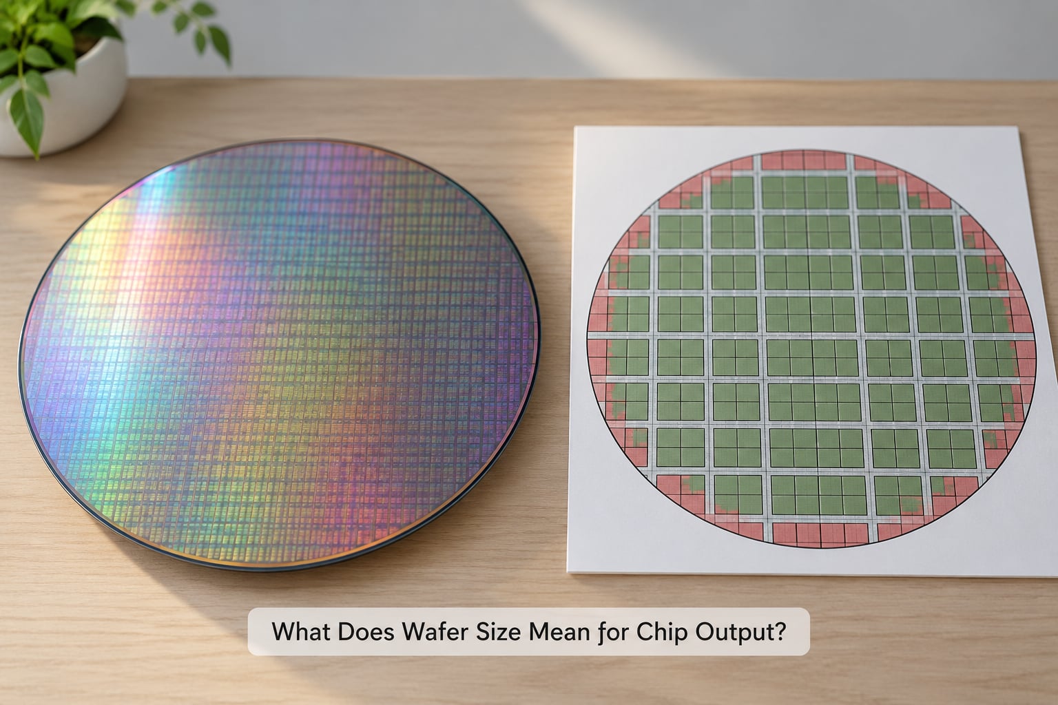
Gross die count is the number of dies that physically fit, ignoring defects. The table below uses one die size, 15mm by 15mm, applied across all four standards so the sizes can be compared directly.
| Wafer size | Wafer area | Gross area vs 100mm | Approx. gross dies at 15mm x 15mm | Multiple vs previous size |
|---|---|---|---|---|
| 100mm (4 inch) | 7,854 mm2 | 1.00x | about 30 | Baseline |
| 150mm (6 inch) | 17,671 mm2 | 2.25x | about 67 | 2.25x |
| 200mm (8 inch) | 31,416 mm2 | 4.00x | about 120 | 1.78x |
| 300mm (12 inch) | 70,686 mm2 | 9.00x | about 260 | 2.25x |
That 2.25x figure is arithmetic, not marketing: 300mm divided by 200mm is 1.5, and 1.5 squared is 2.25. The same maths gives 4x from 100mm to 200mm and 9x from 100mm to 300mm.
Good die counts always fall short of gross die counts, for reasons that have nothing to do with diameter. The outer margin of every wafer is unusable for finished die, and that edge exclusion zone takes a larger bite as diameter shrinks, which is one reason edge loss hurt 100mm proportionally more than it hurts 300mm. Scribe lines between die consume area too. On top of that, random particle defects and yield learning curve losses remove dies until a process has matured.
Defect patterns matter as well. A kill on a small die may land on one part, while a defect in a large die can scrap several neighbours at once, so die size and defect density together set the good-die number.
How Did Larger Wafers Change Semiconductor Equipment?
A wafer size transition is an equipment project before it is a process project. Process tools had to grow proportionally, or a single 300mm wafer simply would not fit through the chamber, the robot or the load port. Semiconductor equipment suppliers responded with wider process kits, heavier wafer handling arms and carriers, and load ports built for FOUPs holding the new format.
Physics gets harder at scale, too. A wider wafer bends and warps more under its own weight, and thermal processing across a larger radius makes it harder to hold a uniform temperature. Spin coating, etch uniformity, chemical mechanical planarisation and anneal profiles all have to be tuned across a bigger surface, and defect inspection coverage takes proportionally longer. Cleanroom handling also gets more delicate because a single particle landing on a larger wafer has more opportunities to land on a die.
Then there is supply. Engineering wafers for ramping a new format are scarce and expensive, because fewer fabs run them, which slows the yield learning curve and makes the first years of any new diameter more expensive per good die than the headline area maths suggests.
Did Moving from 100mm to 300mm Always Reduce Chip Costs?
No. The direction of the cost trend is right, but the timing and the magnitude depend on how full the fab is and how well the process has matured. Larger wafers lower the processing cost per die when fab utilisation is high and yield is already proven, which is the steady state a successful fab eventually reaches.
During the ramp the arithmetic works against you. A new diameter needs new tools, new carriers, new process recipes and a fresh engineering wafer supply. Yield on a newly introduced wafer size starts lower and climbs along a learning curve as defect sources are found and fixed. Edge loss removes a share of the larger wafer’s extra area, and a fab running at low utilisation pays for the same tool time without the die output.
The historical record shows the pattern clearly. 200mm capacity peaked around 2007, contracted hard after the 2008 crisis, and then recovered as mature analog, power and automotive demand filled it again. The same thing happens at any size; the transition is expensive first and cheap later.
That is also why the practical gains are usually quoted as a few percent rather than a multiple. A 2.25x jump in gross area does not become a 2.25x drop in cost per good die, because tooling, cleanroom, overhead and yield losses all scale too.
Are Smaller Wafers Still Used Today?
Yes, and not as a rounding error. 200mm capacity is genuinely in demand in 2026 for mature-node analog, power management, automotive and industrial microcontrollers, image sensors and discrete devices, because those parts do not shrink fast enough to justify rebuilding for 300mm, and automotive qualification cycles reward a process that has already proven itself.
150mm and 100mm lines serve similar roles at smaller scale, and they are also where compound semiconductor work happens. Silicon carbide power devices, gallium nitride RF parts, photonics and certain sensor technologies are produced on 150mm and smaller wafers where crystal growth and tooling economics favour the smaller format.
Research and pilot lines keep using 100mm and 150mm for a simple reason: they are cheap. A process development team can own a small number of 100mm tools instead of a fraction of a 300mm fab, which is why early node and early material learning still happens on small wafers long after volume production has moved on.
What Comes After 300mm Wafers?
450mm is the most studied next step, and it has not happened. The case for it is the same square-law argument: 450mm offers 2.25 times the gross area of 300mm, and consortium materials have quoted around 2.3 times as many chips per wafer once real die-count modelling is applied.
Two industry groups did the engineering work. The Global 450mm Consortium, G450C, studied the equipment and materials implications, and the F450C effort looked at facilities and facility infrastructure. Both concluded the transition needed sustained global demand thresholds before the capital case held, and those thresholds have not been reached consistently.
The practical barriers are heavier than the 300mm transition was. Handling and load port design for a disc that wide becomes a major engineering problem on its own. Warpage and flatness across the larger radius are harder to control, edge exclusion removes a larger absolute area of prime material, and the yield learning curve is longer because more die per wafer means more opportunities for a systematic defect to appear at once.
That has pushed the other idea, stretching rather than stepping. If a fab cannot justify a new diameter, can it run 310mm or 320mm on the tools it already owns? The 1970s move from 2 inch to 2.25 inch wafers by changing only the chuck suggests the idea has merit. In practice, the ecosystem has stayed with 300mm.
Frequently Asked Questions
Is a 300mm wafer the same as a 12-inch wafer?
Not exactly. A 300mm wafer measures 300 millimetres, which is 11.81 inches. The industry calls it a 12-inch wafer because fabs and equipment suppliers standardise on whole-inch labels for the four commercial diameters: 100mm as 4 inch, 150mm as 6 inch, 200mm as 8 inch and 300mm as 12 inch. The 0.19 inch difference is real and shows up in load port and carrier design.
How many chips can fit on a 300mm wafer?
It depends on die size. A 300mm wafer has about 70,686 mm2 of gross area, so a 15mm by 15mm die fits roughly 260 times on the raw area before edge exclusion, scribe lines and defects are removed. Real good-die counts run lower, and the yield learning curve means a fab ramping a new size sees fewer working dies per wafer until the process matures.
Does a 300mm wafer mean the chips use a newer process node?
No. Wafer diameter and process node are unrelated dimensions. Diameter is a physical size in millimetres, set by tooling and fab economics. Node is a feature size in nanometres, set by lithography and process control. A fab can run 300mm wafers at a mature 90nm node for analog parts, and 200mm wafers have been used at nodes far beyond anything most people assume.
Why did the semiconductor industry skip 175mm wafers?
There was never a commercial 175mm standard. Running two diameters at once means two sets of process tools, carriers and recipes, which is the single most expensive mistake a fab can make during a transition. Once 150mm was established and 200mm was clearly needed, the industry jumped directly. The 125mm format is the rare example of an intermediate size adopted on purpose, and it existed for a few years only.
Why are 100mm and 150mm wafers still manufactured?
Because older diameters still fit the work. Analog, power and discrete devices have not shrunk in area fast enough to justify new equipment, so a fully depreciated 150mm or 100mm tool set can hold good fab utilisation and lower cost per die than a fab that just paid for 300mm capacity. Those sizes also dominate compound semiconductor work such as silicon carbide, gallium nitride and photonics, plus research and pilot lines that cannot justify a large fab.
Conclusion
Wafer size evolution was never a single breakthrough. Each step from 100mm to 150mm to 200mm to 300mm happened when device density and demand made the fixed cost of a fab too heavy to spread over too few dies, and each one cost years of tool rebuilds and yield learning before it paid back.
If you are comparing historical process generations or planning modern capacity, start with the diameter timeline and check two things first: the die area you actually need, and whether the fab at that size is running at good utilisation. Diameter decides how much you can fit on a wafer, but die size, edge loss and yield decide what you actually get out of it.