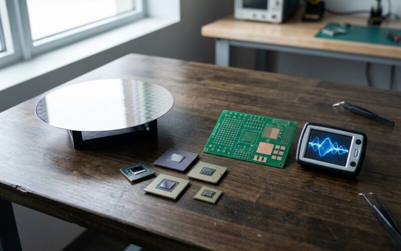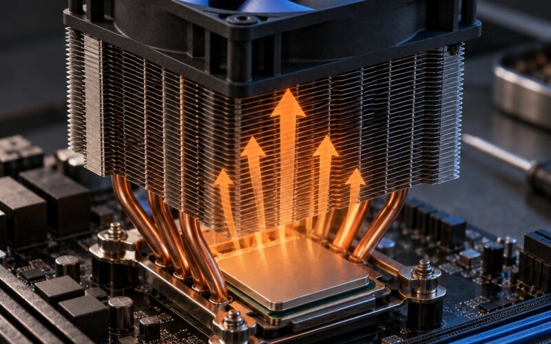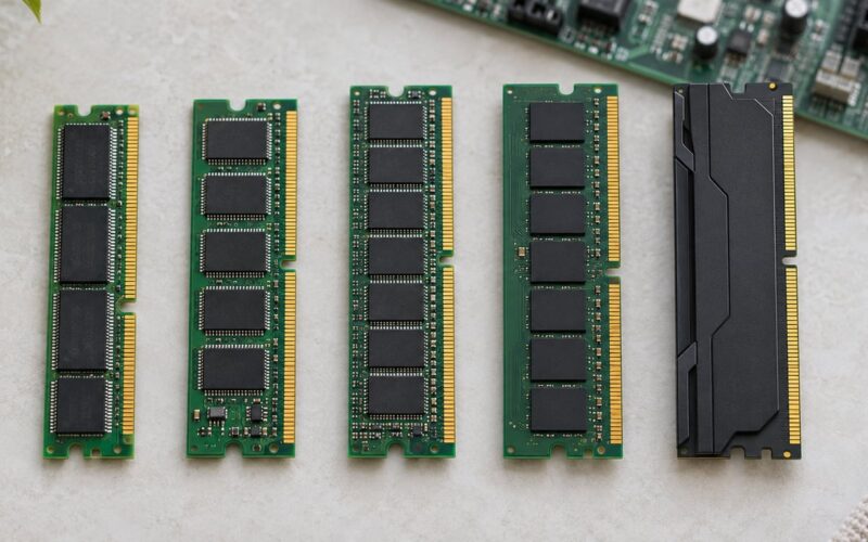
Chip manufacturing is the process of turning raw silicon into working transistors, and nearly every beginner gets stuck on the vocabulary long before they get stuck on the physics. This chip manufacturing glossary for beginners defines the terms you will meet first: wafer, die, fab, foundry, photolithography, reticle, node, yield, chiplet and the rest, each in plain English with a concrete example.
Semiconductor jargon is dense because the industry compresses a lot of physics into three-letter abbreviations. Nobody expects a new hire to know what CMP means on day one, but nobody has time to keep looking it up either. So here is the decoder, organised the way the process actually runs.
A note before we start: this glossary is maintained for 2026, and a few entries shift as the industry moves on. Process node names in particular change every couple of years and rarely mean what they literally say.
Table of Contents
- What Is Chip Manufacturing?
- How Do Engineers Turn a Chip Design into a Physical Chip?
- Core Chip Manufacturing Terms You Should Know
- Materials and the wafer
- Business models
- What Are Wafers, Dies, Nodes, and Process Nodes?
- How to use this chip manufacturing glossary for beginners
- What Are the Main Steps in Semiconductor Fabrication?
- How Do Lithography, Etching, and Deposition Work Together?
- What Are Yield, Defects, and Wafer Sorting?
- What Happens After a Chip Is Fabricated?
- Chip Design and Manufacturing Terms Worth Keeping Handy
- Frequently Asked Questions
- What is chip manufacturing in simple terms?
- What does process node mean in semiconductors?
- What is the difference between a wafer and a die?
- Does a smaller process node always mean a better chip?
- What is lithography used for in chip manufacturing?
- When does a chip design go to tape-out?
- Conclusion: Start with the Manufacturing Flow
What Is Chip Manufacturing?
At its simplest, chip manufacturing is a sequence of five stages: someone designs the circuit, a fab prints that design onto silicon wafers, an assembly house packages the individual dies, test engineers verify them electrically, and the parts ship to whoever builds the product.
The stages below are the ones you will keep hearing about. Every term later in this glossary attaches to one of them.
| Stage | What happens | Key terms |
|---|---|---|
| Design | Circuits are drawn and simulated on a computer before anything physical exists | EDA, PDK, RTL, standard cell, tape-out |
| Wafer fabrication | Layers of film, light and etch build the transistors on a silicon disc | Wafer, lithography, photomask, etching, deposition, CMP |
| Assembly | The wafer is cut up and each die is bonded into a package | Dicing, wire bonding, flip chip, substrate, advanced packaging |
| Test | Chips are probed and stressed to confirm they work | Wafer sort, known-good die, ATE, burn-in, binning |
| Shipment | Packaged parts go to module makers and end products | HBM, chiplet, interposer |
If you remember one chain of words, remember this one: sand becomes ingot, ingot becomes wafer, wafer becomes die, die becomes package, package becomes chip. Everything else in the industry hangs off those five nouns.
How Do Engineers Turn a Chip Design into a Physical Chip?
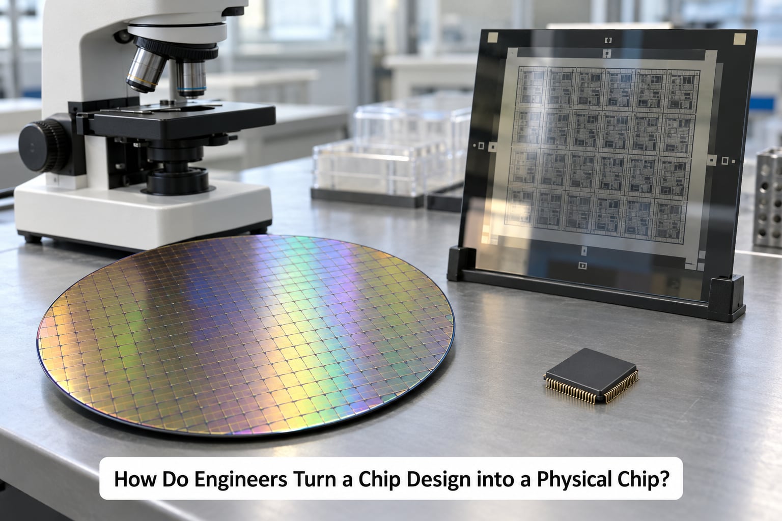
The design exists as a set of database files until tape-out, the moment the finished layout is handed to the foundry and never changes again without enormous cost. After that, a physical process takes over.
- Design verification. The layout is checked against the foundry’s rules for spacing, density and current capacity.
- Mask set creation. Each layer of the circuit is rendered onto a photomask, sometimes called a reticle.
- Wafer processing. The wafer goes through the same deposition, lithography and etch cycle dozens to a hundred-plus times, once per layer.
- Wafer sort. A probe station touches each die with tiny needles and records which ones work.
- Dicing. The wafer is cut along scribe lines into individual dies.
- Assembly. Each good die is bonded to a substrate or interposer and enclosed in a package.
- Final test. The packaged part is retested, sometimes under stress, before it ships.
Steps three through seven are where most of the vocabulary lives, which is why the rest of this guide is organised around them.
Core Chip Manufacturing Terms You Should Know
Materials and the wafer
Semiconductor – a material that conducts electricity somewhere between a metal and a rubber, and whose conductivity you can switch on and off on command. That switchability is the whole point.
Band gap – the energy gap a particle has to cross before it can move freely. Silicon’s band gap sits around 1.1 eV, which is why silicon conducts far less than copper but far more than glass.
Silicon – the workhorse material, refined from quartz sand into purity levels that make chemistry textbooks look careless. Roughly 28 percent of the Earth’s crust is silicon, but almost none of it is usable as-is.
Ingot or boule – the cylinder of pure monocrystalline silicon pulled from molten silicon, often more than a metre long. Wafers are sliced off it like thin coins.
Czochralski method – the standard way to grow an ingot, by touching a seed crystal to the melt and pulling slowly while it rotates. The name is pronounced chuh-KRAH-ski.
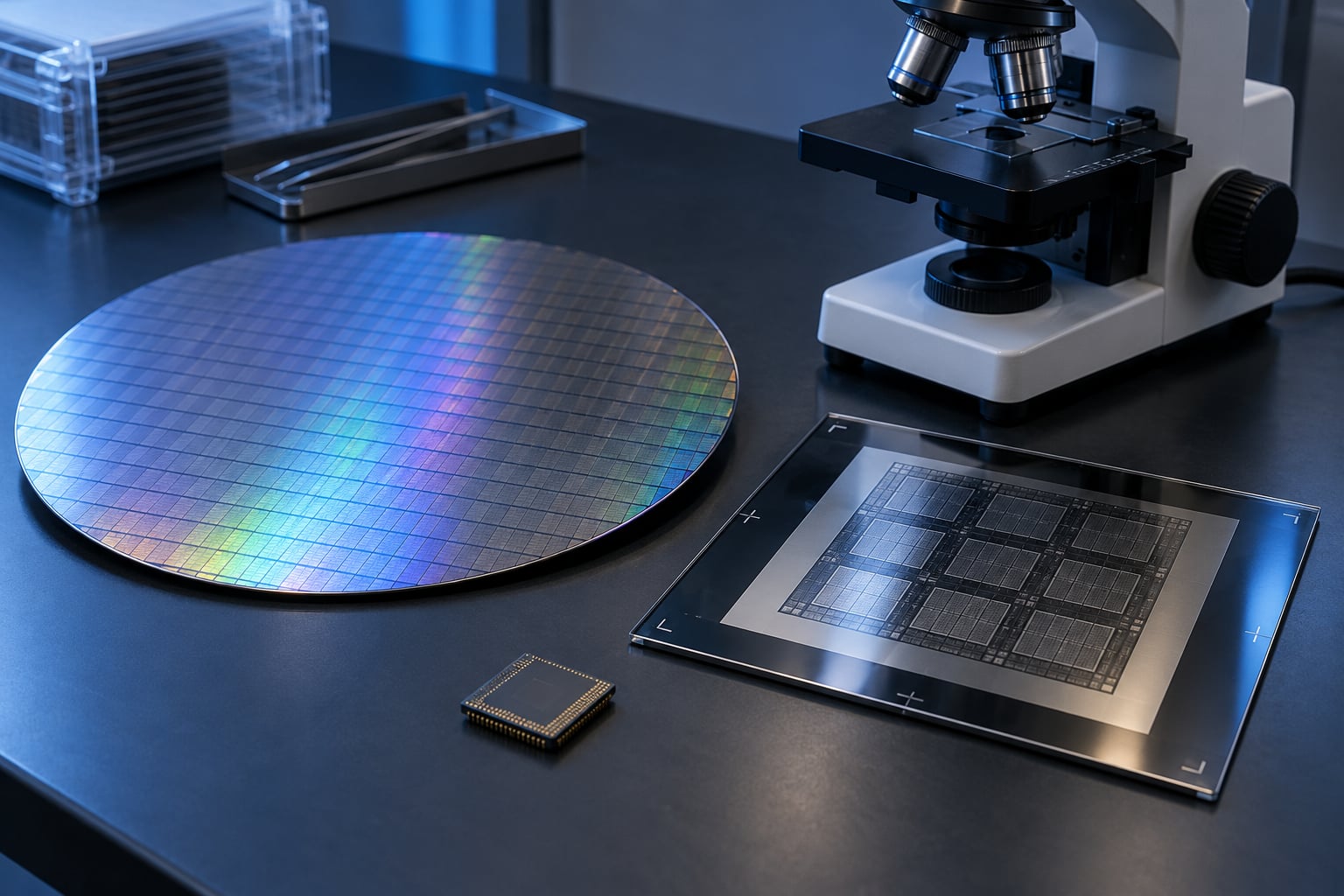
Wafer – the thin circular disc of silicon that hundreds or thousands of identical circuits get printed onto. Common diameters are 200 mm and 300 mm, and a modern wafer is under a millimetre thick.
Bare wafer – a wafer that has been sliced, polished and cleaned but has no circuit pattern on it yet. A finished wafer coming out of the fab is not called bare.
Epitaxy – growing a thin crystal layer on top of an existing wafer so the new layer lines up with the crystal beneath it. The wafer below is called the substrate.
Die – one copy of the circuit pattern on a wafer, before it has been cut free or packaged. A 300 mm wafer holding advanced logic can carry more than a thousand of them.
Transistor – the tiny voltage-controlled switch that stores a bit or gates current. A modern processor holds tens of billions of them.
MOSFET – the specific switch design used for nearly all digital logic, named for its metal-oxide-semiconductor structure. FinFET and gate-all-around are newer shapes of the same idea.
Doping – adding a controlled trace of another element, usually boron or phosphorus, so silicon regions become n-type or p-type and conduct in a controlled way. Doping is what makes a transistor a transistor rather than a lump of rock.
Ion implantation – the machine that does the doping, firing ions of the chosen element into the wafer surface at high energy.
Business models
Fab – short for fabrication plant, the physical building where wafers are processed. It is a facility, not a company, which is where most of the confusion starts.
Foundry – a company that manufactures chips designed by somebody else. TSMC is the clearest example.
Fabless – a chip designer that owns no manufacturing facilities at all. Nvidia and Qualcomm design; foundries build.
IDM – integrated device manufacturer, a company that both designs and fabricates its own chips. Intel and Samsung both operate this way.
OSAT – outsourced assembly and test, a specialist that packages and tests chips for other companies. Amkor and ASE are the big names.
Tape-out – the moment the completed design is released for fabrication. One leading-edge tape-out costs a design team many millions of dollars, which is why engineers treat the schedule like a deadline with no extensions.
What Are Wafers, Dies, Nodes, and Process Nodes?
These four get used interchangeably in news coverage, and they describe four different scales. The table below is the one to memorise.
| Term | What it measures | Typical figure |
|---|---|---|
| Wafer size | The diameter of the whole disc | 200 mm or 300 mm |
| Die size | The area of one circuit copy on the wafer | A few square millimetres for logic |
| Feature size | The smallest printed dimension, such as gate length or metal pitch | Tens of nanometres and below |
| Process node | The name of a generation of process technology | A label like 3nm or 7nm |
The catch is that process node stopped being a physical measurement. A node name is now a marketing label, and two foundries advertising the same node routinely produce chips with different real feature sizes. Node names also no longer track a single dimension, since chipmakers pick whichever feature shrinks most impressively for that generation.
So when you see a launch described as a 3 nm chip, the useful reading is generational: it means a later process than 5 nm, with usually better density and lower energy per switching operation. It does not mean any measured feature is exactly 3 nanometres wide.
How to use this chip manufacturing glossary for beginners
Most beginners read a glossary front to back and forget it. What works better is reading it once alongside a real process flow, then returning to it whenever a document uses a term you skipped. Keep the process order in your head and every term has an anchor point: CMP means nothing until you know it happens between deposition and the next lithography step.
A second habit helps more than memorisation. When you meet an abbreviation, ask what sentence it could stand for. Learning the expansion once, in context, sticks better than forty definitions read in a sitting.
What Are the Main Steps in Semiconductor Fabrication?
The wafer fab runs a repeating cycle that a beginner can group into two families: steps that add material, and steps that remove it. Nearly every layer of a modern chip is built by adding a film, patterning it, removing the unneeded parts, and flattening the surface again.
Deposition adds a thin film. PVD spatters atoms off a target physically, CVD reacts gases on the wafer, and ALD lays down one atomic layer at a time for exceptional control.
Oxidation grows a silicon dioxide layer by exposing silicon to steam or oxygen at high temperature. It is the original way insulators were made, and silicon dioxide remains a key insulating material.
Photoresist is the light-sensitive coating spun onto the wafer before exposure. It is the sacrificial material that records the pattern.
Photolithography projects the circuit pattern through a photomask onto the resist. EUV uses 13.5 nm wavelength light for the smallest features, while DUV uses 193 nm immersion light and still handles most mature production.
Etching removes material. Wet etch uses liquid chemistry; dry or plasma etch uses an ionised gas to cut shapes vertical walls would not allow. Selectivity is the ratio of how fast the intended layer etches compared to the layer underneath it.
CMP, chemical mechanical planarization, is the polishing step that flattens the wafer so the next layer can be printed. It is chemistry plus a moving abrasive surface, and it is the reason layers stack without one short-circuiting into the next.
Ion implantation provides the doping that turns plain silicon regions into n-type or p-type.
Cleaning happens between steps. Even a single stray particle can kill a transistor, so cleaning is constant rather than occasional.
Metrology is the measurement step. CD-SEM images finished features to confirm their size, and overlay targets confirm each new layer lines up with the one beneath it.
Overlay, critical dimension and aspect ratio are the numbers engineers quote when a product falls short of its performance target. Aspect ratio is simply how deep a feature is compared with its width, which is why narrow, deep trenches get difficult fast.
How Do Lithography, Etching, and Deposition Work Together?
Patterning works the same way every time: coat a layer of resist, print the pattern with light, develop the resist, then use it as a stencil for the next operation. The cycle repeats for every layer.
| Order | Step | What it accomplishes |
|---|---|---|
| 1 | Deposition | Lay down a uniform film of the material that will become the layer |
| 2 | Photoresist coat | Spin on a light-sensitive coating |
| 3 | Exposure | Project the mask pattern through the optics onto the resist |
| 4 | Develop | Remove the softened resist where light hit |
| 5 | Etch or plate | Use the hardened resist as a stencil to shape the film |
| 6 | Strip and clean | Clear the resist and prepare a flat surface |
A useful comparison is printed circuit board manufacturing. On a board, the mask says where copper stays and a chemical bath eats everything else away. In a fab, the same idea applies, except the mask is printed with extreme ultraviolet light, the film being removed can be a nanometre thick, and the “bath” is a plasma that has to cut straight through without touching the layer below.
Because each pass adds one layer, the whole sequence is repeated until the circuit is complete. That is why a modern leading-edge process has well over thirty active layers stacked on a single die, and why each one has to land within a tolerance measured in nanometres.
What Are Yield, Defects, and Wafer Sorting?
Yield is the percentage of die on a wafer that function correctly, and it is the number that decides whether a product makes financial sense. A fab that yields 60 percent of its die on a wafer with 900 die gets 540 working chips out of every wafer it processes.
Defect density counts how many defects appear per unit area of wafer. Particle means a contaminant of any size, and a particle landing on a critical pattern is usually the whole story of a bad die.
Defectivity is not the same as yield. A process can have excellent defect density and still lose yield from other causes, and a clean-looking wafer surface can hide critical dimension drift that kills every die. Clean is not the same as yielding well.
Process window is the range of temperature, pressure and chemistry over which the process holds its target dimensions. Wide process windows are easier to run in volume, which is why process engineers spend so much time narrowing process windows and widening them at the same time.
Wafer sort is the probe step where a test machine lands on each die with tiny probes and records what it finds. Binning is sorting those results into performance grades, so a wafer yields a spread of parts rather than one uniform grade.
Known-good die, or KGD, means the die has already passed electrical test before packaging. Confirming a die works beforehand avoids paying for a package that wraps a dead chip.
Yield is also why chiplets changed the conversation. A large monolithic die has more area, so it has more chance of a defect anywhere on it. Smaller dies can be tested separately and only the good ones assembled, which turns yield from a blocker into a design strategy.
What Happens After a Chip Is Fabricated?
Once patterning finishes, the back end of line takes over. The word back end covers everything from wafer thinning through final test, and it is a different set of companies from the fab.
Wafer thinning grinds the wafer down so it can fit into a thin package. Dicing cuts along the scribe lines, with a diamond blade or a laser, separating individual dies. Bumping adds tiny solder or copper pillars to the die surface for later connection.
Wire bonding attaches the die to the substrate with hair-thin gold or copper wires. Flip chip turns the die over and bonds its bumps directly to the substrate, which shortens the electrical path and supports far more connections.
WLP, wafer-level packaging, builds the package on the wafer before dicing so each die arrives with its own package. FCBGA, flip-chip ball grid array, handles large processors and is the most common high-performance approach.
Substrate is the printed board inside the package that carries power and signals. Interposer is a silicon or organic layer that sits between dies and acts as a wiring highway.
Chiplet is a die that does part of a system’s job and is packaged alongside others. Advanced packaging covers the modern techniques, including 2.5D stacking on an interposer and 3D stacking, plus hybrid bonding, where two surfaces are fused directly without solder in between.
HBM, high bandwidth memory, is DRAM stacked vertically and bonded beside the logic die, which is how AI accelerators get the memory bandwidth they need. UCIe is an open standard for connecting chiplets to each other.
Testing comes in two distinct stages, and the difference matters when you read a quality report.
| Stage | When it happens | What it checks |
|---|---|---|
| Wafer-level test | After patterning, before dicing | Whether each die functions electrically |
| Final test | After packaging | Whether the whole part meets its specifications in its real configuration |
ATE, automated test equipment, runs the final test. Burn-in stresses parts at elevated temperature and voltage for hours so early-life failures show up before the product ships rather than in the field.
Chip Design and Manufacturing Terms Worth Keeping Handy
These terms live on the design side but decide how the manufacturing side behaves, which is why they show up in every factory meeting.
EDA – electronic design automation, the software used to draw, simulate and verify circuits. PDK – process design kit, the foundry’s library of standard cells and rules for one process node.
IP core – a prebuilt block of verified logic licensed into a design, such as a memory controller or a SerDes. Standard cell – a library of simple precharacterised logic blocks the tool assembles into a larger circuit.
RTL – register-transfer level, the behavioural description of a circuit that exists before physical layout. Design-for-manufacturability means designing so the process can build it reliably, mainly by respecting spacing and density rules.
The acronym decoder below covers the ones that show up most often in job postings, meeting invitations and supply-chain documents.
| Acronym | What it stands for | In one line |
|---|---|---|
| EDA | Electronic design automation | The software that draws and verifies circuits |
| PDK | Process design kit | A foundry’s rulebook and cell library for one node |
| DRC | Design rule check | Automatic verification that the layout obeys process rules |
| LRC | Lithography restricted design | Layout rules for features the scanner cannot reliably print |
| OPC | Optical proximity correction | Software that pre-distorts the mask so the printed shape matches intent |
| CD | Critical dimension | A feature size the process must hit precisely |
| SEM | Scanning electron microscope | The imaging tool used to measure finished features |
| SIMS | Secondary ion mass spectrometry | Measures how much dopant landed in the silicon |
| ATE | Automated test equipment | The system that electrically tests finished parts |
| BGA | Ball grid array | A package type with an array of solder balls underneath |
| QFN | Quad flat no-lead | A small package with contacts on all four sides |
| SoC | System on chip | Many functional blocks on one die |
| SiP | System in package | Several dies packaged together as one part |
| FPGA | Field programmable gate array | A reconfigurable chip sold as general-purpose hardware |
| ASIC | Application-specific integrated circuit | A chip built for one specific job |
| MEMS | Microelectromechanical systems | Moving microscopic structures used as sensors |
| SiC | Silicon carbide | A wide-bandgap material for high-voltage and high-temperature work |
| GaN | Gallium nitride | A wide-bandgap material common in RF and fast chargers |
| InP | Indium phosphide | The substrate behind most optical fibre-integrated chips |
| CMOS | Complementary metal-oxide semiconductor | The standard logic process pairing p-type and n-type devices |
| ILD | Interlayer dielectric | The insulating material between metal layers |
| TSV | Through-silicon via | A vertical conductor through a thinned wafer |
| UCIe | Universal chiplet interconnect express | An open standard for die-to-die links |
| HBM | High bandwidth memory | Vertically stacked DRAM used next to logic dies |
| MTBF | Mean time between failures | How long a device runs on average before failing |
| ESD | Electrostatic discharge | The static shock that destroys unprotected electronics |
Two entries in that table carry traps for beginners. RF means radio frequency in most chip contexts but refers to a resistor in another context, so always check which one is meant. And a node name such as 3nm is a generation label, not a measured feature, no matter how precisely it is written.
Frequently Asked Questions
What is chip manufacturing in simple terms?
Chip manufacturing turns silicon into working transistors in five stages. Engineers design the circuit on a computer, a foundry prints that design onto silicon wafers inside a fab, an assembly house cuts the wafer into dies and bonds each one into a package, test engineers verify the parts electrically, and the good ones ship to product makers. Every term in this glossary attaches to one of those five stages.
What does process node mean in semiconductors?
A process node is the name of a generation of manufacturing technology, such as 3nm or 7nm. It describes a whole set of improvements rather than a single physical measurement. Two foundries using the same node name often produce chips with different real feature sizes, so node is best read as a generational marker for density and energy efficiency rather than a literal dimension.
What is the difference between a wafer and a die?
A wafer is the whole round disc of silicon, typically 200 mm or 300 mm across and under a millimetre thick. A die is one individual copy of a circuit printed onto that disc. A single wafer holds anywhere from a few hundred to well over a thousand dies, and each die is cut free and packaged separately before it becomes a chip.
Does a smaller process node always mean a better chip?
No. A smaller node label usually brings higher transistor density and lower energy per switching operation, but that is only one variable. Chip quality also depends on the specific process, memory and analog design, cooling, packaging, and the software running on it. Comparing two chips purely by node number ignores most of what determines real-world performance.
What is lithography used for in chip manufacturing?
Lithography is the step that defines where each layer of a circuit goes. A photomask carrying the pattern is projected onto a light-sensitive coating called photoresist, and where light hits, the resist becomes resistant to the chemical etch that follows. The pattern left behind then guides how the layer is shaped. Every transistor layer on the wafer is built this way, dozens of times over.
When does a chip design go to tape-out?
Tape-out happens when the finished layout is released to the foundry for fabrication, and the design stops changing. Before that point engineers iterate freely against simulation and verification results. After it, any correction means respinning the design and paying for a new mask set and wafer run, which on a leading-edge node costs a design team many millions. That is why tape-out is treated as an unmoveable deadline.
Conclusion: Start with the Manufacturing Flow
If you take nothing else from this chip manufacturing glossary for beginners, hold on to the sequence. Silicon is refined into an ingot, sliced into wafers, patterned by lithography and etch, sorted for working dies, diced, packaged and tested. Every other term describes one step inside that chain.
Your next step is simple. Pick one document you actually read, a product page, a job description or a supply-chain briefing note, and mark every term in it that you cannot explain out loud. That list is a far better study guide than a glossary read front to back, because it is built from the vocabulary your job actually uses.