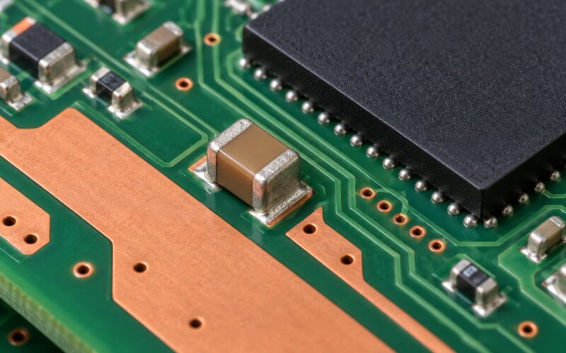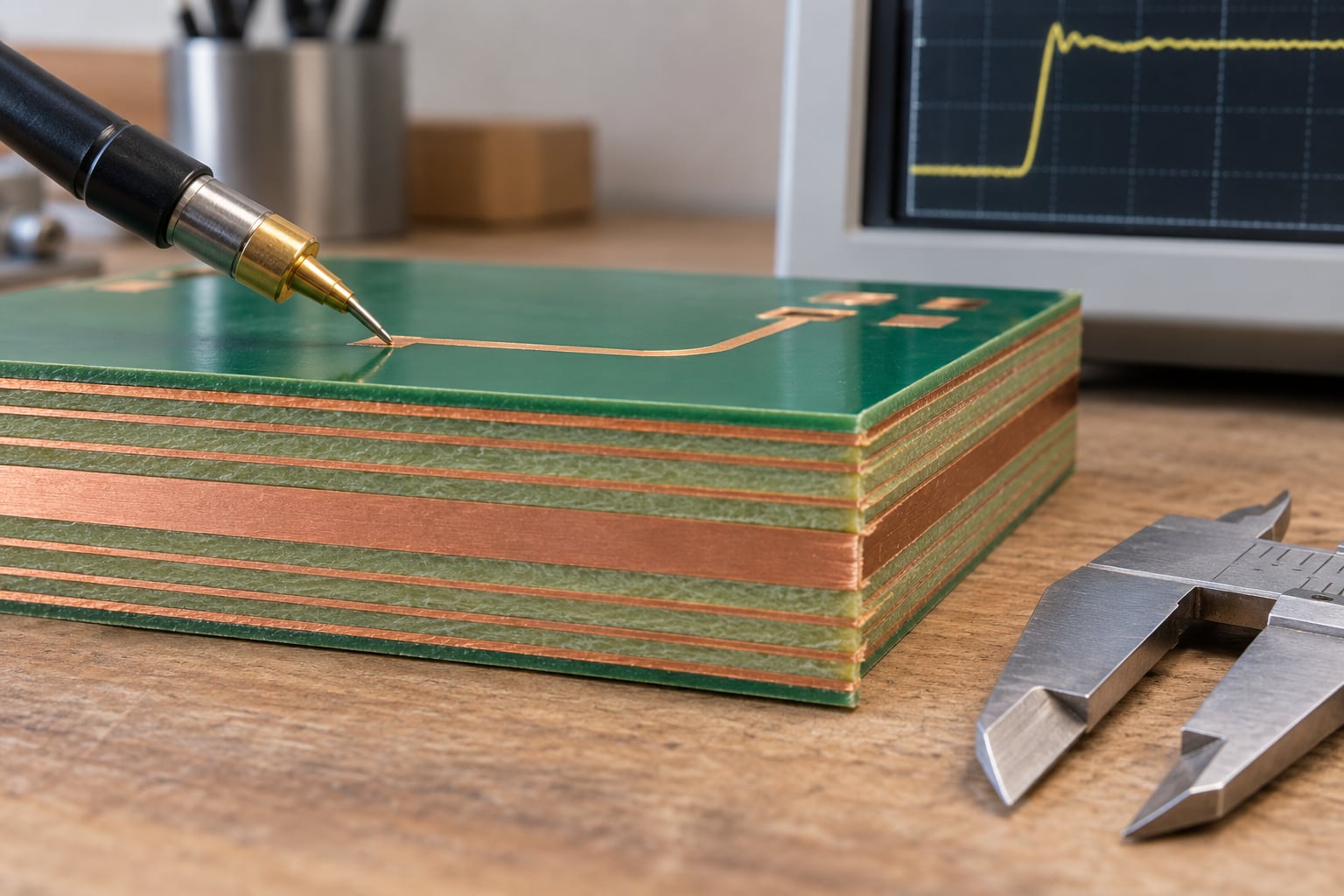
Controlled impedance means you pick the impedance your net needs, choose a real fabrication stack-up, and size every trace so that value holds after pressing, etching and plating. The work is a workflow, not a single formula: define the impedance class, lock the stack-up, calculate geometry against that stack-up, apply constraints in CAD, handle vias and layer changes deliberately, then hand the fabricator a drawing that says exactly what has to be measured and to what tolerance.
This guide walks through that workflow step by step. It assumes you can reach a field solver and you have a fabricator willing to share stack-up data, which is the normal case for anything above a few gigabits per second.
If your board mixes fast digital links with sensitive analog front ends, the impedance classes are only one half of the problem. What mixed signal design is: a guide for engineers covers the partitioning side, which is worth reading before you fix any trace widths.
Table of Contents
- What You Need Before You Route a Single Trace
- Design inputs
- CAD and solver capability
- Stack-up data from the fabricator
- Reference documents and tolerances
- Fabrication documentation
- Step-by-Step Controlled Impedance PCB Design Guide
- 1. Define the required impedance classes
- 2. Choose a fabrication stackup
- 3. Calculate trace and gap geometry for the controlled impedance PCB
- 4. Apply rules across the CAD layout
- 5. Control vias, pads and layer transitions
- 6. Review return paths and plane connectivity
- 7. Validate with simulation and design checks
- 8. Prepare fabrication and assembly documentation
- 9. Verify the fabricated boards
- Common Mistakes in Controlled Impedance PCB Design
- Frequently Asked Questions
- What PCB impedance tolerance should I specify?
- Should differential impedance be calculated from trace width or gap first?
- Why does controlled impedance require a known PCB stackup?
- Do vias significantly affect controlled-impedance traces?
- Can a PCB manufacturer change the impedance if its process is qualified?
- How is controlled impedance verified on a fabricated PCB?
- Conclusion
What You Need Before You Route a Single Trace
Most impedance failures trace back to missing inputs rather than bad arithmetic. Gather the following first.
Design inputs
For each net that matters, you need the target impedance, the tolerance, and the edge rate it runs at. Take those from the interface specification where one exists, and record the document name and revision so the fabricator can see where the number came from.
CAD and solver capability
You need a constraint-driven layout tool that can enforce width and gap rules by net class, plus a 2D or 3D field solver to extract impedance from real geometry. IPC-2141A gives the closed-form equations for microstrip and stripline; the field solver is what catches the cases those equations do not cover, such as coupled pairs, vias and pads in the field.
Stack-up data from the fabricator
Ask for the proposed stack-up in writing before you start: layer count and order, core and prepreg material with nominal dielectric constant and dissipation factor, finished dielectric thickness, copper weight on each layer, and the final pressed board thickness. Nominal values from a datasheet are a starting point. The fabricator’s process limits are what your calculation has to sit inside.
Reference documents and tolerances
Keep IPC-2141A for impedance calculation methods, IPC-2221 for general design practice, and IPC-6012E for the acceptance requirements a Class 2 fabricator works to. Have a calculator or field-solver model ready so you can reproduce every number the fabricator quotes back at you.
Fabrication documentation
Have the drawing template ready with impedance callouts, a net class table, coupon requirements and a deviation process. Doing this at the end is when contradictory widths appear on the same layer, and that is the single most common cause of a production hold.
Step-by-Step Controlled Impedance PCB Design Guide
1. Define the required impedance classes
Sort every net into classes before touching geometry: impedance-critical, length-matched but not impedance-critical, and unconstrained. Typical targets are 50 ohms single-ended and 90 or 100 ohms differential, but the interface specification wins over any convention.
Record for each class the target value, the tolerance percentage, the signal edge rate and the reference document. Then decide how the net will be implemented, because surface microstrip, embedded microstrip, stripline and co-planar waveguide are not interchangeable at the same width.
If rise-time data is missing, derive it. The usual trigger for treating a trace as a transmission line is when its propagation delay approaches a small fraction of the signal rise time, commonly one-sixth to one-third. Anything longer than that on a fast edge needs controlled impedance.
2. Choose a fabrication stackup
Choose the stack-up from the fabricator’s documented options, not from a generic eight-layer default. Each stack-up has a known dielectric constant, a known dielectric thickness and known copper weights, and your trace geometry will be calculated against those exact numbers.
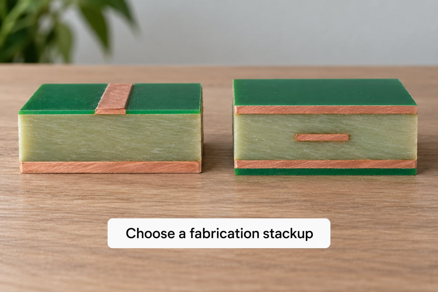
Symmetry matters more than layer count. A build that is not symmetric about its centre warps during pressing, and a warped board changes both dielectric thickness and copper position relative to the reference plane.
| Construction | Where the trace sits | EMI immunity | Routing density | Notes |
|---|---|---|---|---|
| 2-layer microstrip | Outer surface | Low | High | Cheapest to build, widest traces, most sensitive to etch variation |
| 4-layer microstrip | Outer surface over a plane | Medium | High | Most common choice for single-ended and moderate-speed links |
| 4-layer stripline | Inner layer between planes | High | Medium | Buried between planes, so less etch and plating sensitivity |
| 6-layer mixed | Two inner, two outer | Medium to high | Medium | Strictly symmetric; fast nets move to the inner layers |
| 8-layer embedded microstrip | Buried between two dielectrics | High | Low | Most stable geometry, most expensive process |
Keep the reference plane continuous and put impedance-critical routing on the layers with the most predictable geometry. Buried traces see less etch and plating variation than surface traces, so many designs put 25 Gbps and faster links on internal layers.
3. Calculate trace and gap geometry for the controlled impedance PCB
Calculate from the stack-up you actually have: trace width, dielectric height to the reference plane, copper thickness and the material’s dielectric constant. Start with the IPC-2141A equations for a first pass, then run the same geometry through a field solver and use the field-solver result.
Sensitivity is steep enough that rough numbers matter. On common FR-4 constructions, adding one thousandth of an inch to trace width shifts single-ended impedance by roughly 2 ohms, and widening the dielectric gap under a trace lowers impedance rather than raising it. A differential pair is more forgiving on width but reacts to coupling, so gap and width have to be solved together.
Do not treat the nominal value as the delivered value. The fabricator will etch to a compensated width, and the pressed dielectric thickness will land somewhere inside a tolerance band. Build a small budget: nominal width, etch compensation, dielectric thickness tolerance, copper weight variation and the Dk spread of the material. If your nominal value sits on top of the tolerance band, half your boards will fail the coupon. The typical swing on a nominal Dk value of 4.3 across a material lot is on the order of plus or minus 0.2, which alone can move impedance by several ohms.
4. Apply rules across the CAD layout
Turn your calculated geometry into reusable constraints by net class: a width rule, a gap rule, a length-matching rule and a layer-transition rule. That way every member of the class is routed identically by construction rather than by hand.
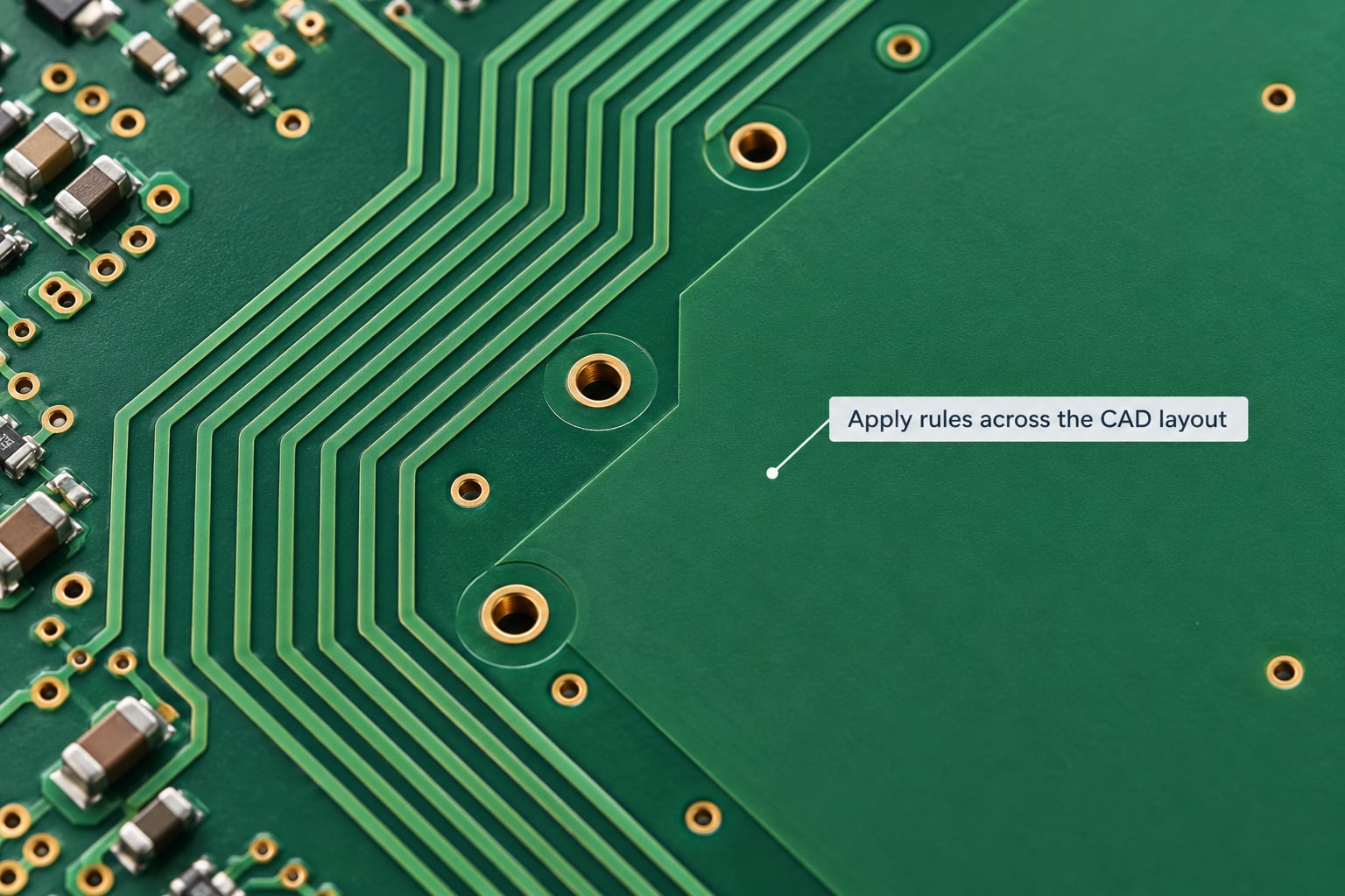
Route differential pairs edge-coupled with the calculated gap held constant, and keep the pair coupled over its whole run. Pairs that wander apart and come back together lose coupling and pick up skew along the way. Use arc or rounded corners instead of sharp right angles, because a 90 degree corner on a fast edge excites the adjacent traces.
Keep a physical isolation gap from unrelated nets, and keep switching or high-current paths off impedance-critical layers. Where you deliberately break a rule, write the reason in the layout notes and tell the fabricator. Silent exceptions are what turn into mismatched coupon results later.
5. Control vias, pads and layer transitions
A via is the most common discontinuity in an otherwise controlled trace. The barrel is a short piece of transmission line with its own impedance, and the anti-pad removes a small amount of plane around it. If the via’s impedance does not match the trace, you get a reflection at every transition, and repeated in a dense layer change the reflections add up.
Three things reduce it. Use the largest via that your layer-transition geometry allows, so the barrel and the trace impedance are closer together. Backdrill the stub when the layer change leaves unused barrel length, since an open stub radiates and rings at its resonant frequency. And where a layer change must be symmetric, change both members of a differential pair together with matched antipads.
Pay attention to stub length. The commonly used rule is that a stub whose electrical length stays well below the rising edge causes negligible reflection, and that threshold shrinks fast as data rates climb. Where you cannot hit it, a pair of anti-pads and a pair of backdrilled barrels on the pair members will do more for the eye diagram than any amount of length tuning. This is the discontinuity that field experience across high-speed links treats as the usual suspect when a fast link has reflections that no width change will fix.
6. Review return paths and plane connectivity
Every high-speed signal needs an uninterrupted return path directly beneath it. That path is the high-frequency continuation of the signal, and when it breaks, the trace radiates into the board, coupling noise to neighbours and radiating externally.
Split planes are the usual culprit. A plane split under a signal forces the return current to detour around the slot, and that detour raises the loop area exactly where you can least afford it. Place splits where no fast net crosses, or bridge them with a capacitor so the return path survives the split at high frequency.
Stitch the plane around board edges and along high-current boundaries with ground vias on a pitch short enough to be useless as a resonant cavity. Where the system or EMC requirements call for a keepout, define it as a rule rather than a hand-drawn area so it survives edits. Design rules around sensitive nodes are worth reviewing alongside ESD protection in chip design explained, since clamping devices near a fast link introduce their own discontinuities.
7. Validate with simulation and design checks
Run the field solver over the finished geometry, not over the initial estimate. Extract impedance for each impedance class and read the result against the tolerance band, then run the constraint checks to confirm no net escaped its class.
Look at the worst cases specifically: the tightest coupled pair, the narrowest trace, the via cluster, the layer with the least reference-plane clearance. Where a result is out of band, adjust the geometry and re-extract rather than accepting it. Preserve the extraction report with the design package; when a board later fails measurement, that report is the fastest way to prove whether the geometry or the process moved.
8. Prepare fabrication and assembly documentation
Put the requirements on the drawing in a form a fabricator can act on without emailing you:
- A net class table: every impedance-critical net, its target value and its tolerance.
- The stack-up you want, by name or by layer table, with dielectric materials and thicknesses.
- The tolerance definition, including whether it is measured on a coupon or on the assembled board.
- The measurement method requested, and where on the board the coupon sits.
- Length-matching tolerances for pairs, specified separately from impedance tolerance.
- Any approved deviation, in writing, with the reason.
State one width per impedance per layer. Two engineers specifying 50 ohms on the same layer with different widths will produce a conflict at the fabricator’s CAM review, and production stops until it is resolved. Assemblers need the same information, including which nets must not be routed through an assembly jumper or test pad.
9. Verify the fabricated boards
Verification happens on a coupon: a set of representative trace geometries built on the same panel with the same process, then measured with time-domain reflectometry or, less often, a vector network analyzer. A coupon tells you whether the process held your geometry, which is a different question from whether your calculation was right.
Check a TDR report by reading the trace, not the pass or fail stamp. You want to see the reported impedance values per coupon net, where on the panel they were taken, and whether the trace is flat or wandering. Measurement near a panel edge picks up process variation that a centre measurement does not, which is why fabricators report both when a result is marginal.
If a reading falls outside tolerance, work through it in order. First confirm the stack-up used on that build matched the one you specified. Then compare the measured value with the nominal to see the direction and size of the shift. Then ask the fabricator for the etch compensation and final pressed dielectric thickness on that panel. The usual causes are a wider-than-nominal dielectric, a stack-up substitution, or a Dk lot outside the band your calculation assumed.
One practical note from engineers sourcing boards overseas: agreeing the stack-up up front does not make the measurement optional. The final reading still drifts, so keep the coupon result with the build record and compare panels to the same order.
Common Mistakes in Controlled Impedance PCB Design
Specifying width without a stack-up. A width is only meaningful against a dielectric height and a material. Give the stack-up first, then the width. One width per impedance per layer is the rule that keeps CAM from bouncing the job.
Asking for five percent tolerance by default. Ten percent is the common default and it matches most interface budgets. Tightening to five percent narrows the process window, which shows up as a higher scrap rate on coupons and boards and can push the order out to a wider review. Specify five percent only where the interface budget genuinely needs it.
Ignoring the via stub. An unused barrel on a layer change is an open stub, and it rings. Backdrill it. This is also the fix that most often gets skipped on boards where the layer-transition problem only shows up as unexplained reflections at the receiver, and the same discontinuity-thinking applies as in fan out wafer level packaging explained, where stub length drives reflections for the same reason.
Splitting a plane under a fast net. The return current detours and radiates. Move the split, or bridge it.
Ignoring solder mask. The mask sits mostly on the wide plane areas rather than on the narrow trace, so the trace itself stays nearly the same thickness. A fabricator will still ask whether you want mask compensation applied, so answer explicitly instead of leaving it to assumption.
Trusting nominal dielectric constant. Material datasheets list a nominal value and a test method. Calculate with the fabricator’s process value, and keep the difference in your tolerance budget.
Before you release artwork, run one short pass: every impedance-critical net is in a net class; every class has a target and tolerance; the stack-up on the drawing matches the one you calculated with; there is one width per impedance per layer; vias have anti-pads sized to the stack-up and backdrilling is called out where the stub is long; every fast net has a continuous return path with no split under it; the length-matching rule is separate from the impedance rule; and the coupon and measurement method are specified. If all eight check out, the remaining risk sits with the process, not the design.
Frequently Asked Questions
What PCB impedance tolerance should I specify?
Ten percent is the common default and matches most interface budgets. Specify five percent only where the interface budget genuinely requires it, because a narrower window shows up as coupon and board scrap rather than as a better impedance. Always state the tolerance per net class and state whether it is measured on a coupon or on the assembled board.
Should differential impedance be calculated from trace width or gap first?
Neither in isolation. Differential impedance depends on both trace width and the gap between the pair, because the coupling between traces sets the even and odd mode values. Solve the pair as a coupled structure, usually with a field solver, and hold the gap constant along the run so the coupling and therefore the impedance stay constant.
Why does controlled impedance require a known PCB stackup?
Impedance is set by trace width, dielectric height, copper thickness and the material’s dielectric constant. The dielectric height and the material come from the stack-up, so without it there is no number to calculate against. If the fabricator presses a different stack-up than you assumed, the finished geometry differs and so does the impedance.
Do vias significantly affect controlled-impedance traces?
Yes, and repeatedly. Each via introduces a barrel and an anti-pad whose impedance differs from the trace, which produces a reflection at every layer change. Using the largest via the design allows, keeping anti-pads within the stack-up rules and backdrilling unused barrel length all reduce the discontinuity. A dense layer change concentrates many of them on one net.
Can a PCB manufacturer change the impedance if its process is qualified?
They can build the qualified stack-up or propose another one, but they should not change it silently. A qualified process has documented dielectric thicknesses, copper weights and material properties, and your calculation depends on those values. If a substitution is proposed, have the impedance recalculated against the new stack-up before you accept it.
How is controlled impedance verified on a fabricated PCB?
On a test coupon built on the same panel with the same process. A time-domain reflectometer measures each coupon trace and reports the impedance, and the fabricator supplies that report with the shipment. Review the values, the measurement locations and the TDR trace shape, not only the pass or fail stamp. A coupon confirms the process held your geometry.
Conclusion
Start with the requirement, not the geometry: list the nets that need impedance, their targets and their tolerances, and pull those values from the interface specification. Then get a real stack-up from the fabricator with dielectric thickness and material properties in writing, calculate trace widths and gaps against that stack-up with a field solver, and hold a tolerance budget so your nominal value sits in the middle of the band.
Everything after that is discipline rather than calculation: constraints in CAD, deliberate via and layer-transition geometry, continuous return paths, and drawing notes a fabricator can act on without emailing you. Do that and a coupon measurement becomes confirmation, not diagnosis.