A chip takes roughly two to four years to go from a written specification to a product in volume production, and only about three to four months of that is spent inside the fab actually manufacturing wafers. If you are asking how long it takes to make a chip from design to silicon, the honest answer is that design dominates the schedule, and fabrication is the visible but shorter part.
The confusion comes from mixing four different milestones: design completion, tapeout, first silicon and production readiness. They land months apart, and each one triggers a new queue, a new cost and often a respin. Here is how the schedule actually breaks down.
Table of Contents
- How Long Does It Take from Design to Silicon?
- What Does the Design-to-Silicon Process Include?
- How Long Each Major Stage Takes
- How Long It Takes to Make a Chip from Design to Silicon
- Why Chip Timelines Differ by Process Node
- What Is Tapeout and Why Does It Matter?
- How Long from Tapeout to First Silicon?
- How Much Faster Is a Mature-Node Chip?
- Can the Design-to-Silicon Timeline Be Shortened?
- Frequently Asked Questions
- Can a chip be designed and fabricated in less than six months?
- What is the difference between tapeout and first silicon?
- How long does it take to manufacture a chip after tapeout?
- Does first silicon mean the chip is ready for mass production?
- How long does chip packaging add to the design-to-silicon schedule?
- What is the fastest realistic path from chip idea to working prototype?
- Conclusion: Build the Schedule from the First Requirements
How Long Does It Take from Design to Silicon?
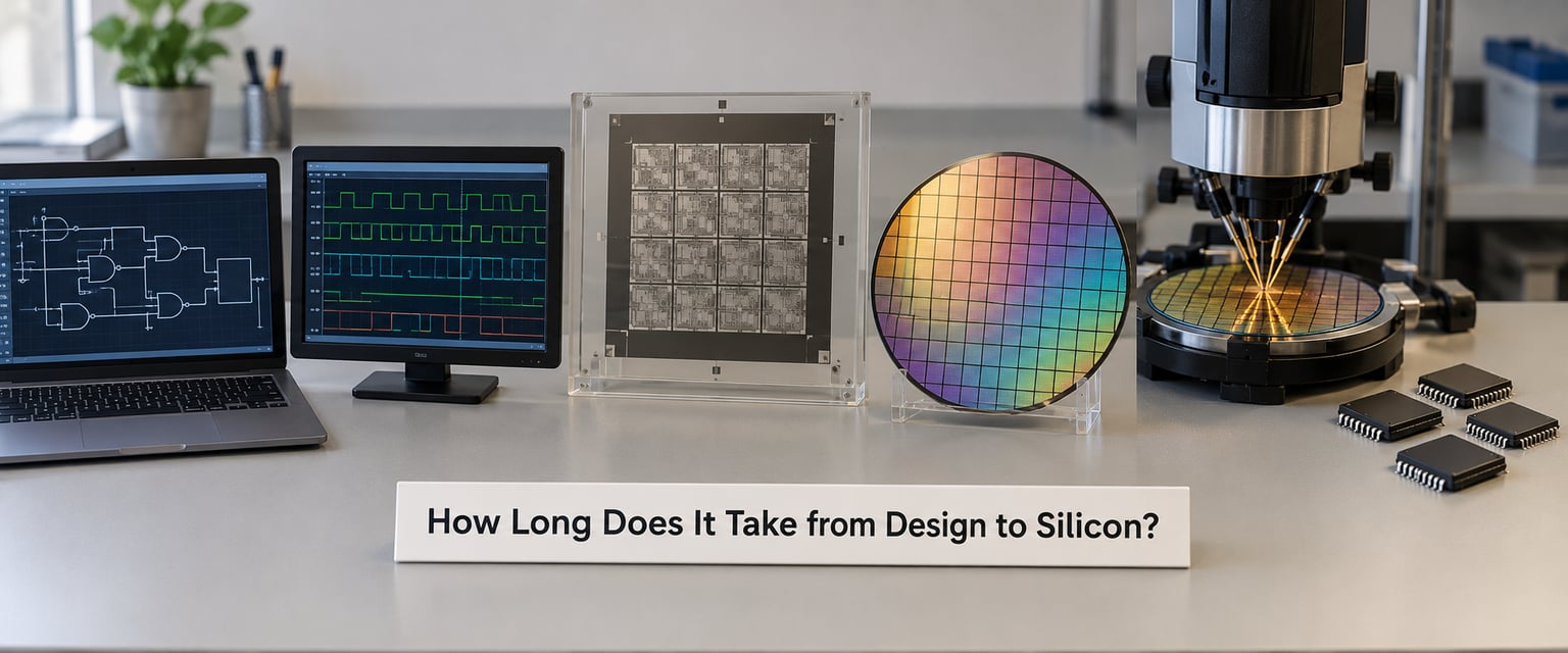
End to end, plan on two to four years for a leading-edge chip, twelve to eighteen months for a straightforward design on a mature or mid-range node, and six to nine months for a small design team using AI-accelerated EDA flows and proven IP.
The single most useful table in chip planning looks like this. Durations overlap, so the columns do not sum to the total.
| Stage | Typical duration | Who owns it | Main bottleneck |
|---|---|---|---|
| Specification and architecture | 1 to 3 months | Design team | Getting requirements to stop moving |
| RTL design | 3 to 9 months | Design team | Reusing IP instead of writing it |
| Verification and simulation | 3 to 12 months, runs alongside RTL | Design team | Debugging, often up to a third of the schedule |
| Synthesis, place and route, sign-off | 3 to 6 months | Design team and EDA tools | Timing closure on a congested netlist |
| Tapeout and mask set | 2 to 6 weeks | Foundry and mask shop | Mask write and inspection |
| Wafer fabrication | 3 to 4 months | Foundry | Cycle time plus capacity queue |
| Wafer probe and dicing | 1 to 3 weeks | Test house | Probe card build for a new die |
| Packaging and test | 1 to 3 months | OSAT or in-house | Substrate and assembly capacity |
| Validation, respins, yield ramp | 3 to 18 months | Both parties | Finding bugs and ramping good-die output |
GlobalFoundries has described a single wafer run as roughly 700 process steps spread across 60 or more layers, taking about three months from start to finish. That figure is the part everyone quotes, and it is the smallest block on a modern chip project.
What Does the Design-to-Silicon Process Include?
Design-to-silicon covers everything from the first architecture decision to a batch of tested, packaged dies that have come out of the line. It ends when you have working silicon in hand, not when the chip ships.
Inside that boundary you get specification, architecture, RTL, verification, synthesis, place and route, sign-off, tapeout, mask fabrication, wafer fabrication, wafer probe, dicing and packaging. Every one of those stages can hand the project back to an earlier stage.
Outside the boundary sit board design, firmware bring-up, system validation, customer qualification and volume production. Those often take as long as the chip itself, which is why a four-year program for a flagship processor still delivers a product years after the first RTL file was committed.
How Long Each Major Stage Takes
Requirements and architecture usually take one to three months for a well-briefed program and considerably longer when the product definition is still moving. Mobile SoC and AI accelerator projects sit at the slow end, automotive and industrial parts at the fast end because the requirements are fixed years in advance.
RTL design runs three to nine months for a design that leans on licensed processor cores, interface IP and library cells. A team writing everything from scratch adds months. Practitioners on r/chipdesign describe three to four months from spec to layout for a first-time designer, with layout itself taking one to two months on top.
Verification is scheduled in parallel from day one but consumes the largest single block of engineering time. One widely cited figure from an EDA engineer put debugging at up to 37 percent of the chip design timeline. That is why simulation environments and formal checks are staffed early rather than after layout.
Implementation converts the netlist into layout: synthesis, floorplanning, place and route, timing closure, physical verification, DFT and scan insertion, then sign-off against timing, power and DRC rules. Expect three to six months here, and expect several loops between place and route and timing analysis because the flow is serial and stop-and-go.
Tapeout to production then runs on someone else’s schedule. The foundry builds the mask set, fabricates wafers, probes them, ships dies to the assembly house, and the package comes back for test. Validation follows, and any bug at this point triggers a respin that repeats everything from tapeout onward.
How Long It Takes to Make a Chip from Design to Silicon
Here is a concrete 26-month schedule for a mid-range accelerator built by a team of about 40 engineers, starting from an approved specification.
| Month | What is happening | Milestone |
|---|---|---|
| 0 to 2 | Requirements, microarchitecture, IP selection | Specification frozen |
| 2 to 9 | RTL bring-up alongside a growing verification environment | RTL feature complete at month 9 |
| 6 to 12 | Back-end verification and corner-case debugging | Verification sign-off at month 12 |
| 10 to 15 | Synthesis, place and route, timing closure loops | Design sign-off at month 15 |
| 15 | Tapeout, GDSII released, mask set ordered | Tapeout |
| 17 to 20 | Wafer fabrication, roughly 700 steps | Wafers out |
| 20 to 21 | Wafer probe, yield read, die shipment | First silicon at month 21 |
| 21 to 23 | Packaging and system bring-up | Boards running the chip |
| 23 to 26 | Validation, one respin resolved, yield ramp | Production release at month 26 |
Four dates matter for planning: design completion, tapeout, first silicon and production readiness. In the schedule above they fall at months 15, 15, 21 and 26. Reporting against first silicon alone hides five months of work that follows it.
Why Chip Timelines Differ by Process Node
The process node drives most of the variation. A 180 nm analog part and a 3 nm AI accelerator share a vocabulary but not a schedule.
Design complexity is the first difference. Leading-edge SoCs use far more logic, larger memories and far more interconnect, and each of those blocks brings its own verification burden. Mature-node analog and power devices have few digital blocks, and the layout is often small enough for a handful of designers to hold in their heads.
Mask count follows. Each additional lithography layer means another mask to write, inspect and correct, which lengthens both mask preparation and the fab cycle itself. Advanced nodes with EUV layers and complex interconnect stacks carry far more of them than a mature process.
Process complexity and capacity do the rest. Each wafer repeats hundreds of deposition, etch, implant and lithography cycles, and the number of times the wafer returns to a given tool determines how long it takes. Leading-edge capacity is also scarce, so a slot in the queue can add weeks before a single wafer starts moving.
What Is Tapeout and Why Does It Matter?
Tapeout is the point where a finished design database, usually delivered as GDSII or the foundry’s equivalent format, is released for manufacturing. The foundry takes that frozen database and produces a set of photomasks, or reticles, one per layer.
Calling it a freeze is accurate. After tapeout the layout is fixed, so any change means a new mask set and a new wafer run. Designers on r/chipdesign are blunt about this: a chip design very rarely works fully at the first tapeout, and teams plan for respins as a matter of course.
Not every tapeout is the same. A preliminary or MPW tapeout places the design on a shared wafer with other customers to get early data cheaply, which is useful for a first look but gives a small lot and a long queue. A final tapeout is a dedicated lot, costs far more, and is the one that feeds volume production.
Scheduling-wise, tapeout is the commitment point. Mask set cost scales with layer count and node, and capacity must be reserved before the run starts, so moving the date by a month usually means renegotiating with the foundry, not just shifting an internal milestone.
How Long from Tapeout to First Silicon?
From tapeout to first working silicon usually runs four to seven months. Mask production and inspection take two to six weeks, wafer fabrication adds three to four months, and probe plus packaging adds another six to ten weeks.
| Process technology | Mask set | Wafer fabrication | Probe and package | Tapeout to first silicon |
|---|---|---|---|---|
| Mature node, 180 nm to 65 nm | 2 to 4 weeks | 1 to 2 months | 3 to 6 weeks | 3 to 4 months |
| Mid-range, 40 nm to 28 nm | 3 to 5 weeks | 2 to 3 months | 4 to 8 weeks | 4 to 5 months |
| Advanced FinFET, 16 nm to 7 nm | 4 to 8 weeks | 3 to 4 months | 6 to 10 weeks | 5 to 7 months |
| Leading edge, 3 nm and 2 nm | 6 to 12 weeks | 3 to 4 months, queue dependent | 8 to 12 weeks | 6 to 9 months |
Delays usually come from four places: mask corrections discovered during inspection, capacity queue time before the lot starts, wafer probe results that force a functional issue, and packaging slots. In an AI accelerator program the packaging step has become the constraint more often than the wafer step, because high-bandwidth memory stacks and advanced substrates are harder to source than wafers are to order.
How Much Faster Is a Mature-Node Chip?
A mature-node chip typically reaches first silicon two to four months sooner than a leading-edge design, and often reaches volume production inside a year rather than two or more. Design is faster too: fewer layers to verify, smaller mask sets to pay for, and processes that most teams already know.
That speed is not free. Mature processes give you larger transistors, more leakage, worse performance per watt and fewer options for on-chip memory density and high-speed interfaces. A 65 nm part will sit comfortably in an automotive or industrial socket; it will not compete with a 3 nm part on compute density.
For analog, power and mixed-signal devices in SiC or GaN, where performance comes from device physics rather than density, the mature node is often the right answer anyway. The shorter schedule is a side benefit, not a compromise.
Can the Design-to-Silicon Timeline Be Shortened?
Some stages compress well. Others are physics and queue time, and no amount of engineering effort moves them.
- Reuse verified IP. Licensed processor cores, SerDes, memory controllers and interface blocks cut months from RTL and verification. This is the single biggest lever available to a small team.
- Start from a platform design. A proven chip family gives you a working baseline, so the program becomes a derivative rather than a first design.
- Use multiproject wafer services. Sharing a wafer with other projects cuts mask cost and shortens the wait for early silicon, at the price of a small lot.
- Prototype in an FPGA first. RTL that runs on an FPGA before tapeout catches a surprising share of logic bugs without a mask set.
- Run verification in parallel. Building the verification environment alongside RTL, rather than after, is the practical answer to the 37 percent debugging figure.
- Engage the foundry early. Design rule decks and process design kits change. Teams that review against the current deck before layout save a respin.
- Plan capacity and packaging early. Queue position and assembly slots are booked months ahead; finding out late adds weeks you cannot engineer away.
- Use AI-accelerated flows where the tool supports it. One vendor reports traditional concept-to-silicon at 12 to 18 months against 6 to 9 months for teams using AI-assisted RTL generation and cloud-native flows. Treat that as the low end of the range, not the new normal.
Frequently Asked Questions
Can a chip be designed and fabricated in less than six months?
Yes, for a small design on a mature node using proven IP, a multiproject wafer and a team that has taped out before. Six months is not realistic for a leading-edge SoC, a large die or anything needing significant respins. The practical floor for most programs is nine to twelve months.
What is the difference between tapeout and first silicon?
Tapeout is the moment the finished layout is released to the foundry for mask production, and it freezes the design. First silicon is the moment tested dies come back from the line. Between them sit mask fabrication, roughly 700 wafer process steps, wafer probe and packaging, usually four to seven months.
How long does it take to manufacture a chip after tapeout?
Three to four months of that is wafer fabrication alone, which is the part most articles quote. Add two to six weeks for masks, one to three weeks for wafer probe, and six to ten weeks for packaging and test. Full tapeout-to-silicon therefore lands between three and nine months depending on node.
Does first silicon mean the chip is ready for mass production?
No. First silicon means the design is manufacturable and testable, not that it is correct or cheap to build. Teams typically spend three to eighteen months after first silicon on validation, bug fixes, respins and yield ramp before a production release, and yield, not capacity, decides when volume shipments begin.
How long does chip packaging add to the design-to-silicon schedule?
Packaging and test normally add one to three months after wafers are probed. That figure has stretched for AI accelerators, where high-bandwidth memory stacks and advanced substrates are in short supply, and packaging is now often the binding constraint instead of the wafer itself.
What is the fastest realistic path from chip idea to working prototype?
For logic, tape out a small design on a mature node through a multiproject wafer: roughly three to four months of design, then three to four months to silicon. For algorithms and interfaces, skip silicon entirely and map them onto an FPGA, which can be running in weeks and often becomes the prototype that ships alongside the ASIC.
Conclusion: Build the Schedule from the First Requirements
The schedule for how long it takes to make a chip from design to silicon is decided long before anyone enters a fab. Design and verification take six to eighteen months, wafer fabrication takes three to four, and validation and yield ramp take another three to eighteen on top.
Start planning from four numbers: the target process node, the date you intend to tape out, the foundry lead time you have been quoted, and the volume you need to hit. Everything else on the schedule is a dependency between those four.