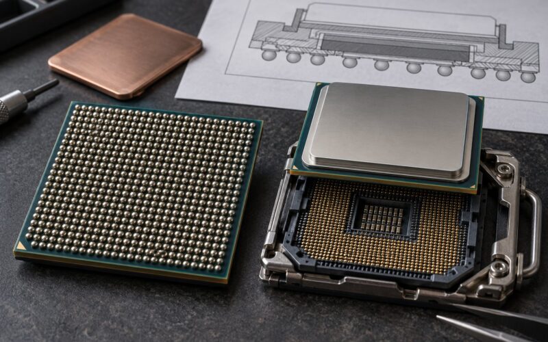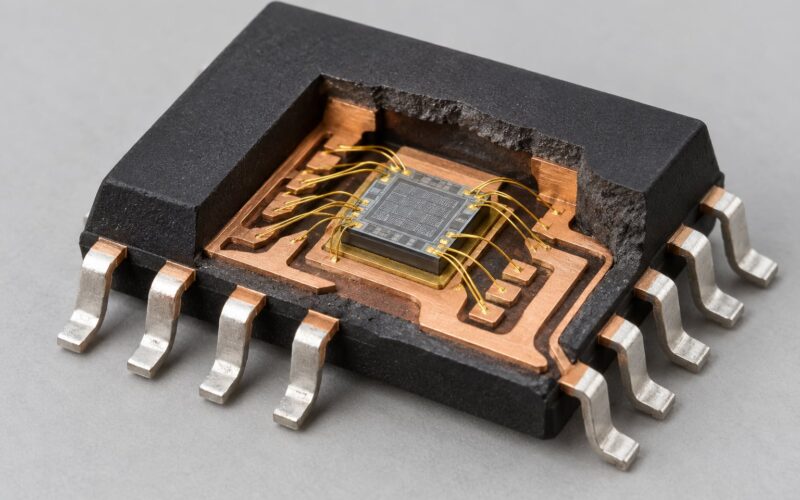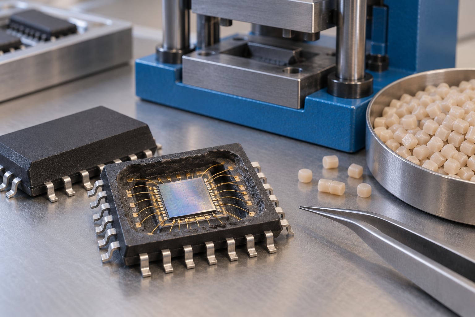
Mold compound in chip packaging is the thermosetting epoxy injected over a die and its bond wires to permanently seal the assembly. You will usually see it called epoxy molding compound (EMC), and it is sold as a heavily silica-filled material. It supports the die mechanically, blocks moisture and contaminants, carries heat out of the silicon, and electrically isolates the die from everything around it.
That definition hides a lot. The same material decides whether a package warpages on the board, whether it passes a humidity reliability test, and how much signal loss a high-speed part sees. Get the formulation wrong and you rework the whole assembly flow.
Below is the working version: what the material is made of, how it is molded, why it shrinks, how it fails, and how engineers actually choose one.
Table of Contents
- What Is Mold Compound in Chip Packaging?
- Why Chip Packages Use Encapsulation
- How Mold Compound Is Made
- The Main Types of Epoxy Molding Compound
- Mold compound in chip packaging for high-frequency and radiation-sensitive parts
- How Mold Compound Is Applied During Packaging
- What Fillers Do in Mold Compound
- Cure Shrinkage, Warpage, and Package Stress
- Thermal, Electrical, and Moisture Performance
- How Engineers Select the Right Compound
- Transfer Molding, Compression Molding, and Other Processes
- Common Mold Compound Problems and Test Methods
- Frequently Asked Questions
- What is mold compound made of?
- Is epoxy mold compound toxic or hazardous to handle?
- Does mold compound conduct heat well?
- What is the difference between mold compound and underfill?
- How long does mold compound have a shelf life?
- Why does molded compound need a post-mold bake?
- Conclusion: Start With the Package Requirements
What Is Mold Compound in Chip Packaging?
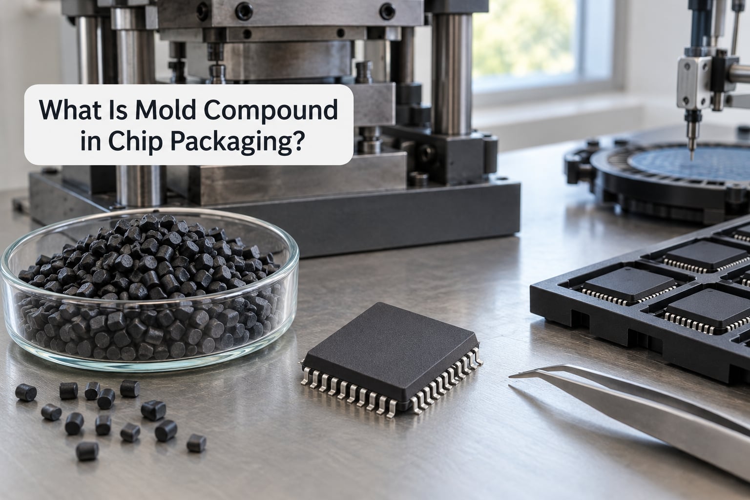
Mold compound is the encapsulating material that becomes the body of a molded semiconductor package. A B-staged pellet is placed in a heated multi-cavity tool, softened, and forced by a plunger around the die, the leadframe and the wires, then cured so it becomes a rigid thermoset. The die sits at the center of that body, mechanically supported for the rest of its life.
It is worth separating the four neighboring materials that people mix up constantly:
- Die attach is the adhesive, solder or sintered silver that bonds the die to the leadframe or substrate. It handles heat conduction at the die interface, not protection.
- Underfill is a liquid epoxy dispensed capillary-style into the gap under a flip-chip die, then cured. It fills a narrow space; mold compound fills the whole package body.
- Glob top is a liquid resin dropped over a die to form a protective dome, common in memory and wafer-level work where the compound is not injected.
- Conformal coating is a thin sprayed or dipped layer for board-level corrosion protection, not a structural package body.
Mold compound is the one in that family that gets injected under pressure into a steel tool. Everything else is dispensed, cured in place, or applied as a thin film.
Why Chip Packages Use Encapsulation
A bare die is fragile in ways that are easy to underestimate. Silicon is brittle, the bond wires are 15 to 25 micrometers of gold or copper, and the passivation on top is a few hundred nanometers of oxide. None of that survives handling, board assembly, or a humidity soak on its own.
Encapsulation does four jobs at once:
- Mechanical. The compound becomes a rigid shell that carries the load instead of the wire bonds, and it absorbs vibration and drop energy across the whole body rather than concentrating it at a single joint.
- Electrical. Epoxy is a good insulator, so the die surface is isolated from the leads, the mold tooling and the environment.
- Thermal. The package body is a heat spreader. Filler and resin together move heat from the die out to the board or heat sink.
- Environmental. The body blocks moisture, ionic contamination, dust and handling damage, and it is what makes a moisture sensitivity level rating meaningful.
Encapsulation is also what allows a die to be tested electrically after molding. A molded body stays attached through final test, so probing happens on finished, protected parts rather than on bare silicon.
How Mold Compound Is Made
EMC starts as a formulation and ends as a solid pellet. The formulation is mostly resin and filler by weight, with a smaller set of additives that control cure speed, adhesion and appearance.
| Component | What it does |
|---|---|
| Epoxy resin | The structural network. Usually an epoxy cresol novolac, or a biphenyl-type variant chosen for lower moisture uptake. |
| Curing agent (hardener) | The stoichiometric reaction partner. Typically a phenolic resin or an anhydride that crosslinks with the epoxy groups. |
| Accelerator or catalyst | Sets how fast gelation happens inside the mold, which is what lets the part reach ejection strength in under a minute. |
| Spherical silica filler | Sets the coefficient of thermal expansion (CTE), adds thermal conductivity, and cuts cure shrinkage. Often above 80% by weight. |
| Flame retardant | Required in many automotive and industrial parts. Brominated or phosphorus-based systems are used against UL flammability ratings. |
| Adhesion promoter | A coupling treatment that improves bonding to the leadframe, the die pad and organic substrates. Weak bonds show up later as delamination. |
| Parting or release agent | Keeps the cured body from bonding to the steel cavity. Release is designed in, not left to luck. |
| Pigment | Carbon black or similar, to give the body color contrast for vision inspection and marking. |
The resin and the hardener are different jobs. The resin is the crosslinkable skeleton with many reactive sites. The hardener is the measured reaction partner that closes the network, and because it is dosed stoichiometrically, the two have to be mixed in a controlled ratio. Get the ratio wrong and you get a soft, under-cured body that never reaches full crosslink density.
Manufacture runs through a B-stage. Resin, hardener, filler and additives are mixed, then heated just enough to let the resin soften and wet the filler while the cure reaction is still slow. That partial reaction is what converts a powder into a handleable, low-bleed pellet. Cool it, grind or granulate it, and you have the pellet the molding machine loads. The time-temperature-transformation (TTT) diagram is the tool engineers use to find this window: too little reaction and the pellet slumps, too much and it will not melt in the mold.
The Main Types of Epoxy Molding Compound
The families below are not marketing labels. Each one is a different balance of resin chemistry, filler loading and additive set, built for a different package constraint.
| Type | Defining trait | Typical use |
|---|---|---|
| Conventional general purpose | Novolac resin, standard filler loading, mold temperature near 175C | Leadframe packages such as QFP, SOIC and TO, general BGA |
| High-temperature | Faster cure and higher service temperature rating | Automotive and industrial parts with elevated ambient requirements |
| Low-stress | Lower modulus, low CTE1, filler tuned for thin sections | Large die, thin packages, clip-bond power devices |
| Flame retardant | Halogenated or phosphorus additive package | Parts with a UL flammability requirement |
| Moisture-resistant | Biphenyl or modified resin with low water uptake and high Tg | MSL-sensitive devices, external exposed packages |
| High thermal conductivity | Alumina or other high-k filler replacing part of the silica | Power devices, LED drivers, wide-bandgap parts |
| Low-alpha | Low-alpha filler, screened to limit alpha particle emission | Radiation-sensitive and imaging devices |
Mold compound in chip packaging for high-frequency and radiation-sensitive parts
Two newer requirements are changing the formulation target. High-speed parts care about dielectric loss, so low-dielectric and low-loss filler systems are being qualified where signal integrity through the package body matters. Radiation-sensitive devices care about alpha emission from the filler itself, which is why low-alpha grades are specified and screened rather than assumed.
Low-alpha compound is a good example of a specification that lives entirely in the datasheet. You ask the supplier for alpha emission levels per unit of material, and you compare them against the sensitivity of the detector. There is no field test to fall back on.
How Mold Compound Is Applied During Packaging
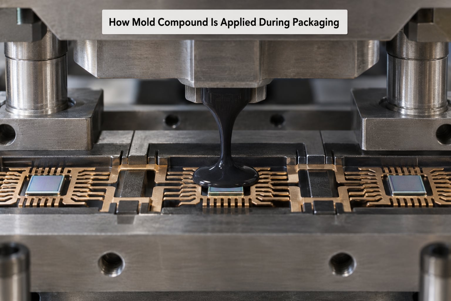
Most molded packages follow a transfer molding sequence. Multi-cavity tools are the reason the process is economical: one press shot fills dozens of packages at once.
- Mold preheat. The chase and cavity reach set temperature, typically around 175C for transfer molding. Mold temperature is the single strongest process lever on the material.
- Die and leadframe load. Wire-bonded or flip-chip assemblies are placed in each cavity, one per site.
- Pellet placement. One pellet per cavity, positioned so the compound front closes over the die last. Placement position is chosen to control the flow front around delicate features.
- Softening. The pellet passes its glass transition temperature (Tg) and drops in viscosity by orders of magnitude, becoming a flowable filled melt.
- Injection. The plunger pushes the melt through the runner system into every cavity in parallel.
- Cavity fill and venting. Air escapes through vents at the far end of the cavity. Blocked vents raise back pressure and cause incomplete fill or flash.
- Cure to gelation. The cure reaction accelerates as temperature rises. Around 40% epoxy conversion, the material passes its gel point and has enough strength to eject. At 150C that takes roughly 100 seconds; at 120C, roughly 350 seconds.
- Eject and finish. The body is ejected, then trimmed, marked, singulated, baked and tested.
Step 8 is where a lot of reliability is actually decided. A post-mold bake at 175C for 3 to 4 hours drives the conversion the mold could not finish, and it is not optional for most parts.
What Fillers Do in Mold Compound
Pure epoxy shrinks a lot when it cures, expands a lot when it warms, and conducts heat poorly. Silica fixes all three problems, which is why filler loading runs above 80% by weight in most formulations.
Two filler details matter more than the rest. First, the particles are spherical, not crushed. A sphere rolls past its neighbors as the melt flows, while an irregular particle interlocks and raises viscosity, so the same loading is possible at a workable flow. Second, the size distribution is multimodal: large spheres carry the bulk loading, smaller ones fill the gaps between them. A narrow distribution forces you to either use very fine powder, which raises viscosity sharply, or accept voids.
More filler is not automatically better. Filler does lower CTE, raise thermal conductivity and cut shrinkage, and it also raises viscosity, makes the melt harder to fill around fine features, and pushes the package closer to a rigid, higher-modulus body that transfers stress to the die and the bond wires instead of absorbing it. Low-stress grades deliberately trade loading for a softer, lower-modulus resin so thin packages can flex rather than crack.
Cure Shrinkage, Warpage, and Package Stress
Cure shrinkage is unavoidable chemistry. As the epoxy network crosslinks, the molecules go from loose and mobile to tightly bonded, and the volume they occupy shrinks. In a package, that shrinkage is constrained by the leadframe and substrate, so it converts into internal stress and visible warpage.
Warpage is really a mismatch problem. Silicon, copper, organic substrate and the filled epoxy each expand by a different amount over temperature. Below Tg the epoxy is stiff and glassy; above Tg it softens and its CTE roughly triples. A package that crosses Tg repeatedly, or that is built from materials with badly mismatched CTE, will bow. Thin packages with large die are the worst case, because there is little body thickness to average the stress out.
Engineers control this with a short list of variables: filler loading and particle size, resin CTE1 below Tg, Tg itself, the mold temperature and cure profile, and the package stackup. Moving Tg up moves the transition above the operating temperature, which removes the biggest discontinuity. Raising filler content and using a lower-modulus resin both reduce the stress that reaches the wire bonds. The cure profile matters too, because faster gelation locks in more residual stress.
Thermal, Electrical, and Moisture Performance
Heat leaves the die through the die attach, the compound, the leads or balls, and the board. Filled epoxy is a mediocre conductor, roughly an order of magnitude below what a metal heat spreader would give, so for power devices the answer is usually a compound formulated with high-conductivity filler, not a thicker body.
Electrically, epoxy is an insulator with a dielectric constant in the low range and a loss factor that is not zero. For ordinary digital parts that never matters. For high-speed designs, the compound sits directly in the signal path, and dielectric loss shows up as insertion loss and as skew between nets.
Moisture is the one that bites. Epoxy absorbs water, and absorbed moisture plus ionic contamination under the body is what drives delamination and the resulting leakage and corrosion failures. This is what a moisture sensitivity level (MSL) rating describes, and it is managed by baking, not by wishful thinking. Compound, leadframes and organic substrates are pre-baked before assembly to remove moisture picked up in storage and shipping, and the post-mold bake after molding serves the cure and the moisture together. Dry cabinets and controlled floor life between bake and assembly matter just as much as the bake itself.
How Engineers Select the Right Compound
Selection starts from the package, not from the material. Define the die size and package thickness, the mold process and temperature you already run, the maximum ambient and junction temperature, the drop and temperature-cycle requirements, and the reliability qualifications you have to pass. Only then compare formulations.
Most decisions resolve in these datasheet fields:
- CTE1 and CTE2. Below and above Tg. Watch the ratio to silicon and to the substrate, not the number alone.
- Tg. Want it comfortably above the highest temperature the part will see, including the reflow and burn-in steps.
- Flexural modulus. The stress lever. Lower values help thin and large-die packages.
- Cure shrinkage. Sets how much of the package geometry you will fight later.
- Filler content. Useful as a sanity check on the density and CTE you expect.
- Viscosity-flow window. Confirms the compound will fill your geometry at your mold temperature in your cycle time.
- Mold temperature and cure time. Must match the process you are qualified on.
- Moisture uptake and MSL. Check the weight gain and the level the compound is rated to.
- Alpha emission. Only if the part is radiation-sensitive.
Then qualify it properly: measure warpage on real packages, run the humidity and temperature-cycle tests your customer requires, and confirm the reliability results with the actual die, substrate and leadframe stackup. Compound behavior is a system property. A compound that passes on one stackup can fail on another, and the datasheet will not tell you that.
Transfer Molding, Compression Molding, and Other Processes
Transfer molding dominates conventional packages. Compression molding serves wafer-level work. Potting is the small-batch fallback. Each trades mold complexity against package geometry.
| Method | Conditions | Fits |
|---|---|---|
| Transfer molding | Mold near 175C, plunger injection, multi-cavity, seconds per shot | Leadframe, BGA, clip-bond power. Highest throughput |
| Compression molding | Mold typically 120 to 150C, press closes and cures the whole wafer at once | Fan-out wafer level packaging (FOWLP) and embedded wafer level BGA (eWLB), where a full-wafer tool is efficient |
| Potting | Room temperature or low temperature fill, long cure | Samples, hermetic and specialty builds. Slow and low volume |
Compression molding runs cooler, which means a slower cure rate and often a material formulated for that cooler window. It also loads the whole wafer in one press stroke, so the economics work out when the die count per wafer is high and the geometry is flat.
Common Mold Compound Problems and Test Methods
Nearly every molding defect traces back to material condition, mold condition or process window. Knowing which of the three to look at first saves a lot of time.
| Defect | Material or process cause | What to change |
|---|---|---|
| Wire sweep | Drag from the advancing, heavily filled compound front across the bond wires | Flow-front design, a lower-viscosity grade, a different pellet placement |
| Voids | Trapped air or moisture, blocked vents, filler agglomerates | Clean vents, pre-bake the compound and frames, check filler dispersion |
| Mold flash | Excess pressure, worn cavity or parting-line mismatch | Check mold fit and clamping; confirm the compound is not over-filling the cavity |
| Incomplete fill | Viscosity too high for the cycle, insufficient mold temperature, starved cavity | Raise mold temperature within the window, lengthen cure, move to a lower-viscosity grade |
| Delamination | Weak adhesion, moisture under the body, CTE mismatch, incomplete post-mold bake | Adhesion-promoted grade, tighter moisture control, verify the bake profile |
| Popcoring | Moisture in the compound turning to steam during the fast thermal ramp | Pre-bake the compound, control floor life, check vent design |
| Warpage | CTE mismatch, residual shrinkage stress, thin package geometry | Shift Tg upward, adjust filler loading and modulus, rebalance the stackup |
| Short or under-cured body | Ejected before enough conversion, or the post-mold bake was skipped | Verify cure time at temperature and the 175C post-mold bake |
Wire sweep deserves its own explanation because the cause is not intuitive. The compound front is a dense, silica-loaded melt moving at speed, and the bond wires stand in its path. The drag bends the wire, and a bent wire under load is a broken wire. It is a flow problem more than a wire problem.
The test methods map to the defect. Cross-sectioning and scanning acoustic microscopy find delamination and voids at the die pad and substrate interfaces. X-ray radiography finds wire sweep and cavity voids. TMA or a scanner picks up warpage, and a moisture soak followed by cross-section is the standard delamination check. Cure state comes from DSC or from a hardness map. X-ray fluorescence on the molded body will tell you whether the right compound went on the part at all.
Frequently Asked Questions
What is mold compound made of?
Mold compound is mostly epoxy resin plus spherical silica filler, usually above 80% by weight. A phenolic or anhydride hardener crosslinks the resin, an accelerator sets the gelation rate, and smaller additive levels handle flame retardancy, adhesion to the leadframe and substrate, mold release, and color. The blend is B-staged into a pellet so the molding machine can feed it consistently.
Is epoxy mold compound toxic or hazardous to handle?
Uncured compound contains epoxy resin and phenolic hardener, which can cause skin sensitization with repeated contact, and it can generate irritant fumes if overheated. You handle it in a ventilation-equipped compounding area with gloves and eye protection, and the fully cured molded part is inert. The more common workplace concern is dust from handling dry powders and pellets, not the finished package.
Does mold compound conduct heat well?
Not on its own. Filled epoxy is a modest conductor, roughly an order of magnitude below metal, so most packages rely on leads, balls and the board to carry heat away. For power devices the material is reworked with high-conductivity filler such as alumina, which raises thermal conductivity but costs viscosity and moldability. Choose based on junction temperature, not on the bulk conductivity number alone.
What is the difference between mold compound and underfill?
Mold compound is injected under pressure to form the whole package body and is supplied as a solid B-staged pellet. Underfill is a liquid epoxy dispensed capillary-style into the small gap between a flip-chip die and its substrate, then cured in place. Underfill handles local stress relief at the bump array; mold compound handles protection, insulation and heat spreading for the entire assembly.
How long does mold compound have a shelf life?
Suppliers specify a shelf life at a stated storage temperature, and it is measured in months rather than years. Storage conditions matter more than the calendar: humidity exposure and repeated temperature cycling change the pellet before molding. Keep compound sealed and dry, log the date code, and pre-bake material before use if it has been open or held through a long floor time. Confirm the current limit on your supplier’s datasheet.
Why does molded compound need a post-mold bake?
The mold cycle only carries the part to roughly 40% epoxy conversion, which is enough for gelation and ejection but not for full properties. A post-mold bake at 175C for 3 to 4 hours completes the crosslinking, which raises Tg, stabilizes the modulus and drives off moisture. Skipping it leaves a package with a lower-than-spec glass transition temperature and a weaker margin on humidity reliability.
Conclusion: Start With the Package Requirements
Start from the package, not the catalog. Define die size, package thickness, substrate material, the mold process and temperature you already run, and the temperature, moisture and drop requirements the part has to survive. Then compare candidate compounds on CTE1 and CTE2, Tg, flexural modulus, cure shrinkage, viscosity-flow window and MSL, and confirm the alpha emission field only if the device is radiation-sensitive.
Finally, validate on real packages with your real stackup. Warpage, humidity soak and temperature cycle will tell you what the datasheet cannot.