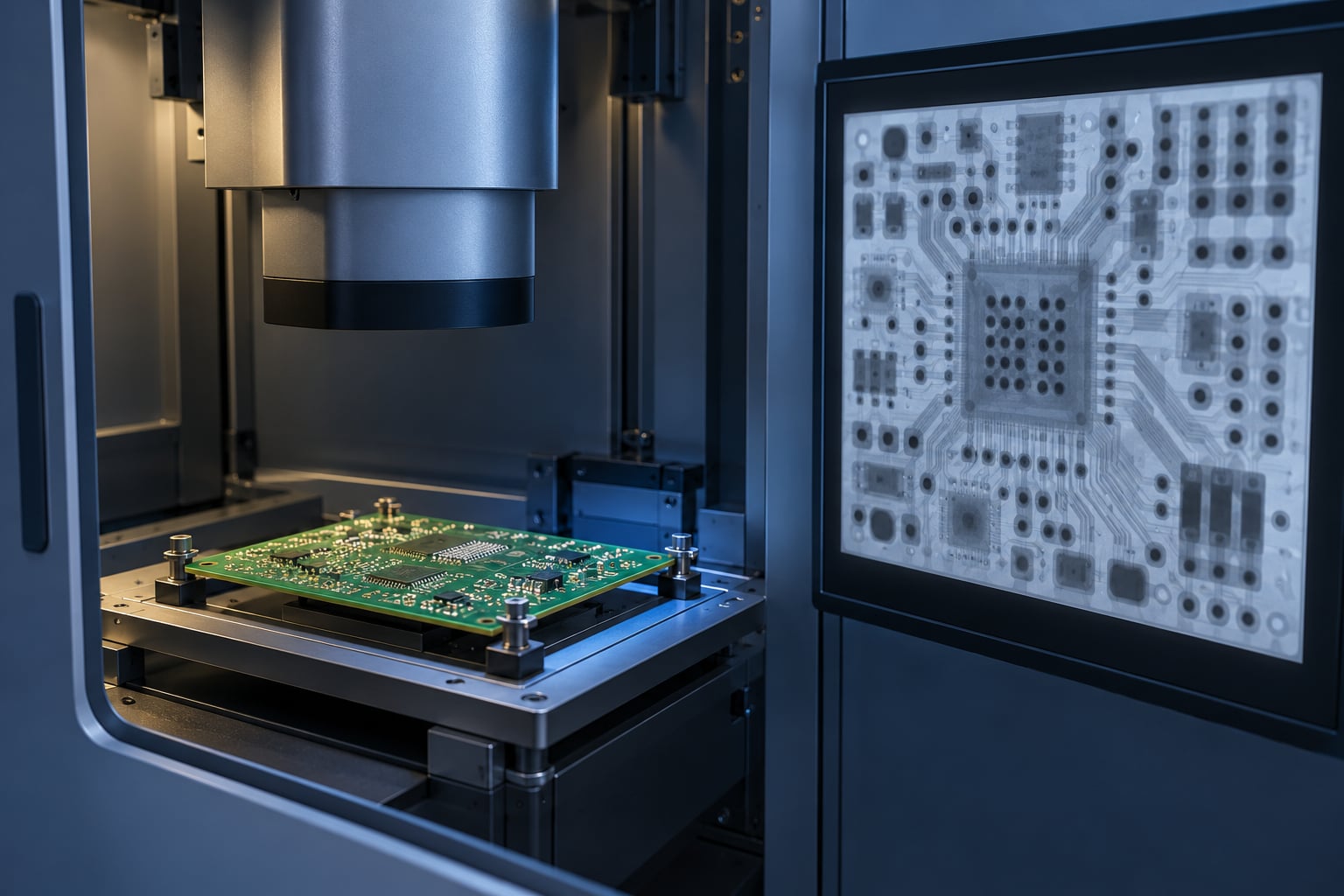
X-ray inspection of electronics is a non-destructive testing method that fires high-energy X-rays through an assembled board and records how each material absorbs them. The result is a picture of the inside: solder joints, copper traces and packages that sit under other parts and can never be seen with a camera or a magnifier.
That matters because modern boards bury their risk. On a ball grid array, most solder joints are physically underneath the silicon, so optical inspection can confirm the package is there and still tell you nothing about whether the joint beneath it formed properly. A void, a bridge or a missing connection that survives visual inspection becomes an intermittent field failure months later.
The rest of this guide covers how the imaging chain works, what the picture can and cannot show, how to choose between 2D radiography and 3D CT, and how engineers turn an image into an acceptance decision. Updated for 2026.
Table of Contents
- What Is X Ray Inspection of Electronics?
- When engineers reach for X-ray instead of a microscope
- How Does X Ray Inspection of Electronics Work?
- What Can X Ray Inspection Reveal?
- Which Type of X Ray Inspection Equipment Is Used?
- How Do 2D X Ray Images Differ from 3D CT Scans?
- How Are Electronics Prepared for X Ray Inspection?
- How Do Engineers Interpret an X Ray Inspection Image?
- What Are the Limits of X Ray Inspection?
- Where Is X Ray Inspection Used in Electronics Manufacturing?
- Frequently Asked Questions
- Does X-ray inspection damage electronics or PCBs?
- What defects can X-ray inspection find in PCBs and packages?
- When should engineers choose 3D CT instead of 2D X-ray inspection?
- Do all electronic assemblies need X-ray inspection?
- Can X-ray inspection replace electrical testing?
- Is X-ray inspection suitable for finding surface defects?
- Conclusion: What to Do First
What Is X Ray Inspection of Electronics?
X-ray inspection is a form of non-destructive radiography: the part is left intact and the image is formed by transmitted radiation rather than by reflected light. Because solder, copper and silicon absorb X-rays differently from epoxy, glass fibre and laminate, that difference is what makes the internal structure visible.
The contrast with optical inspection is the whole point. A camera can see the top of a board, the silkscreen, the polarity marks, the solder fillets at a lead’s heel. It stops at the first opaque surface. X-rays pass straight through the package body, so the joint underneath is in frame on the same image as the components around it. That is why the technique earns its place on line for BGAs, chip scale packages, flip chips and leadless packages such as QFN, where there is no side view to inspect and nothing to remove.
When engineers reach for X-ray instead of a microscope
Engineers reach for X-ray when the suspect joint is concealed, when the defect class is internal rather than surface, or when the failure mode is electrical but the cause is not obvious from the top of the board. Intermittent opens on a fine-pitch package, a joint that failed after thermal cycling, and a burn-in survivor with no visible damage are all classic cases.
It also shows up in places people rarely associate with electronics manufacturing: power modules with die attachments under a moulded body, stacked lithium cells where a dendrite forms inside a sealed pouch, and ceramic substrates whose internal metallisation cannot be probed from outside.
How Does X Ray Inspection of Electronics Work?
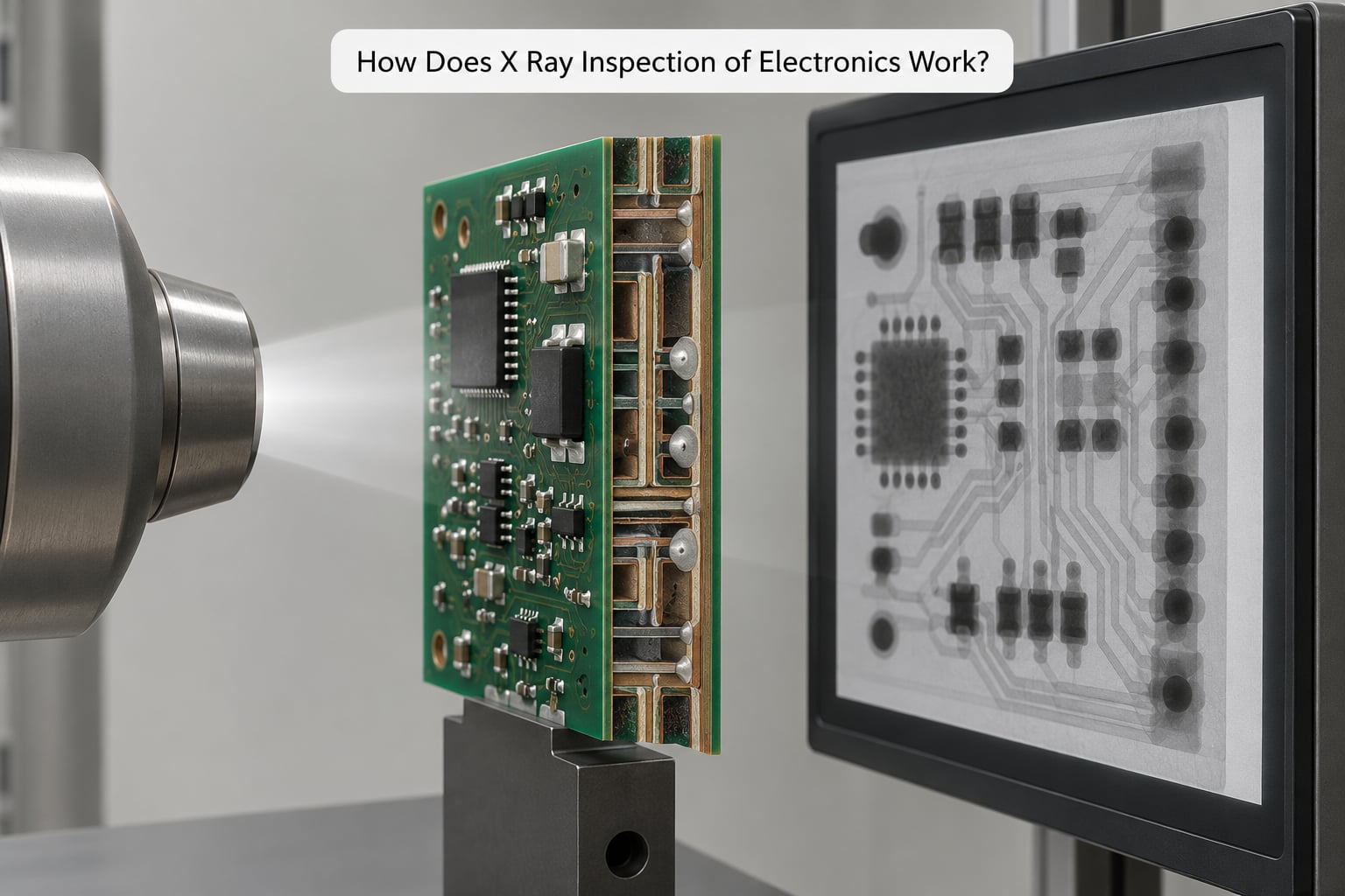
The imaging chain has five stages, and each one is a place where a bad setting shows up later as a bad image.
- Generate the beam. A microfocus X-ray tube heats a small tungsten target to a few thousand kelvin and accelerates electrons toward it. The electrons decelerate on impact and give off X-ray photons with a penetration depth tied to tube voltage. The focal spot is deliberately tiny, often a few micrometres, because a smaller source gives a sharper geometric projection.
- Attenuate through the part. The beam crosses the assembly once. Dense metals (solder, copper, gold) remove far more photons from the stream than resin, laminate or air, so a solder ball shows up as a dark disc against a lighter background. Photon counts drop by roughly the exponential of the material’s linear attenuation coefficient times the thickness it passed through.
- Convert to an electrical signal. A detector sits behind the part. Depending on the system it is a flat-panel scintillator that absorbs X-rays and re-emits visible light for a photodiode array, a high-speed camera looking at a fluorescent screen, or a photodiode array with a columnar scintillator. A high-speed camera system generally resolves fine porosity better than a basic photodiode array, which is why serious void work tends toward that architecture.
- Reconstruct the image. For a single projection the raw frame is already the picture, then contrast, brightness, geometric correction and noise reduction get applied. For CT the sample rotates through several hundred angles, the projections are reconstructed into a voxel volume, and any cross-section or depth view can be pulled out of that volume.
- Measure and decide. Software segments regions, computes void area as a percentage of the projected joint, counts missing or undersized balls, flags bridges where two outlines merge, and writes a pass or fail against the criteria the process engineer set. Results usually log with a board barcode so the failure map can be correlated with process history later.
Two setup decisions change the image more than any software setting. Kilovoltage sets how deep the photons reach, and too little voltage means a thick package looks like a solid block with no internal contrast. Tube current and exposure time set how many photons arrive and therefore how noisy the image is, so operators usually take the longest exposure the cycle time allows rather than the shortest one that keeps up. Copper filters in the beam path strip out low-energy photons that add haze without adding information.
What Can X Ray Inspection Reveal?
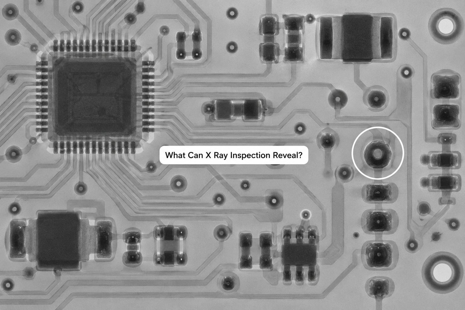
Most of what a quality engineer looks for is a change in the expected shape or density of a known feature. Here is the practical list, with what each finding usually means.
| Finding in the image | What it indicates | Usual cause |
|---|---|---|
| Round lighter region inside a solder ball | Void or porosity in the joint | Moisture or outgassing during reflow, insufficient paste volume |
| Ball outline merging with a neighbour | Solder bridge | Too much paste, pad-to-pad spacing below process capability, poor stencil |
| Ball present but very small | Undersized ball or starved joint | Low paste deposit weight, pad oxidation, incomplete wetting |
| Grid position with no ball at all | Missing ball, open connection | Placement error, dropped ball, pad defect |
| Ball sitting high with a gap under it | Head-in-pillow, insufficient solder fillet | Package co-planarity problem or low solder volume during attach |
| Dull, irregular joint texture | Cold solder joint | Poor wetting, contaminated or oxidised pad |
| Conductive path where none should be | Foreign material, flux residue, dendrite | Contamination, corrosion product, moisture ingress |
| Dark wedge between laminate layers | Delamination or internal void in the board | Press or lamination cycle, resin flow, moisture |
Two of these deserve a note. Head-in-pillow, where a lifted package ball has only a partial contact, reads as a clearly abnormal shape, so it is one of the easier findings to confirm. Voids are more subtle: a small round light area inside a ball is normal, and the question is always how much of the joint’s area it occupies. A lone void tells you the joint is porous; the same void also tells you the joint is carrying current over a smaller cross-section than intended, which is why the threshold question comes up in acceptance discussions.
That is where the most-cited number in this field comes from. IPC-A-610 clause 8.2.12.4 addresses X-ray evidence of solder joint conditions on BGA and similar devices, and the widely applied rule of thumb is a 25 percent limit on the projected void area of a single ball. Class 2 general-purpose electronics is more forgiving than Class 3 high-reliability product. There is a catch worth knowing: no equivalent industry-standard void limit exists for leadless packages such as QFN, which is why you will see shops argue about percentages with nothing to cite. Whichever criteria your process uses, the important part is that they are written down before the line runs, not chosen after a failure.
Which Type of X Ray Inspection Equipment Is Used?
Three families cover almost all electronics work, and the difference comes down to how many viewing angles the system collects.
| Method | Image detail | Dimensional information | Typical speed | Best used for |
|---|---|---|---|---|
| 2D radiography | Good within a single projection; overlap hides layers | Projected area only, no depth | Fastest, seconds per view | Void area, ball count, bridges, first-pass screening on PCBA |
| Computed radiography (2.5D) | Sharp, stored as a digital plate and re-exposed cheaply | Projected, sometimes with tilted views | Fast, with modest handling overhead | Production screening where AOI handles surfaces and X-ray handles joints |
| 3D CT (computed tomography) | Highest; separates features stacked along the beam | True geometry, height, position, density | Slowest, often minutes per region | Failure analysis, package internals, die attach, volumetric porosity |
On the source side, a microfocus tube with a focal spot of roughly one micrometre is the standard for electronics, because geometric magnification depends on that spot size and anything coarser smears the fine features. Nano-focus sources push magnification far higher, into the single-digit micrometre range, and are justified for die-level and wire-bond work where a ball is not the smallest thing you need to see. Focused beam systems and standard medical or industrial sources also appear in the field, and they are adequate for thicker parts such as power modules and castings, where penetration matters more than resolution.
A higher specification is not automatically the right answer. CT on a production line has to move samples through a rotation stage, and that rotation time dominates the cycle. For a high-volume line checking one joint class, a 2D system with an oblique angle and automatic defect recognition usually wins on cost per board. For an engineering lab, CT is worth the time because it answers questions a projection cannot.
How Do 2D X Ray Images Differ from 3D CT Scans?
The gap between 2D and 3D comes down to one fact: a radiograph collapses a three-dimensional object into a single shadow. Everything along the beam path adds up into the same pixel.
That is the 2D limitation, overlap. On a fine-pitch BGA sitting over dense copper, the solder ball shadows and the trace shadows sum together, and a void under one ball can be read as a lighter region belonging to a different feature. Depth is genuinely unknown, not merely hard to see, so a defect can be located laterally with confidence but not vertically. At the same time, a 2D image gives you a projected void area, which is what most acceptance criteria are written against.
CT resolves this by rotating the part and reconstructing a volume. Once you have voxels you can slice through a joint at any height, separate a void inside the ball from a void in the pad below it, measure the actual solder height, and get a density value for each material rather than a single summed grey level. The cost is scan time, mechanical handling of the part, and a much larger data set to store and process.
The practical decision usually goes like this. If the question is “is this joint’s projected void area inside the limit, and are all balls present”, 2D answers it in seconds. If the question is “where exactly is the crack, what fraction of the die attach is bonded, and how deep does the delamination go”, you need 3D. Failure analysis on a returned product is the case where the extra minutes are obviously worth it.
How Are Electronics Prepared for X Ray Inspection?
Good radiographs are made before the part reaches the cabinet. A short preparation routine saves far more time than it costs.
- Identify and log the sample. Record the board or package serial, lot and failure symptom before the part goes under the tube. An image without traceability is a snapshot, not evidence.
- Choose the fixture. A stable holder matters more than a sophisticated one. Foam and low-density tape hold light parts without adding much attenuation; dense metal fixtures add their own image and can hide the feature you came for.
- Set the orientation. Rotate the part to put the suspect joint roughly parallel to the detector, and consider a second oblique view. Tilt separates features that stack in a straight-on projection and costs only a second exposure.
- Pick the parameters. Raise kV until the package is transparent; increase current and exposure until the image is clean; add copper filtering to cut haze. Then zoom in far enough to resolve the smallest ball, and no further, because magnification also magnifies noise and geometric distortion.
- Calibrate and verify. Check the detector offset and the stage position against a known-good reference. A grid artefact or a half-pixel shift will produce convincing false features.
- Handle radiation properly. X-ray inspection systems are operated only by trained personnel under the manufacturer’s procedures. That means interlocked shielding, dosimetry where the site requires it, and never a bypassed interlock. On lead-free assemblies the shielding is part of the equipment design, not an optional add-on.
Preparation also covers dose. A single production inspection is brief, but some devices are genuinely sensitive to accumulated ionising dose: certain CMOS image sensors, some optical components, and a handful of specialty parts have published dose limits. Where a part is known to be dose-sensitive, the operator should use the lowest exposure that still resolves the feature and confirm the total dose against the part’s specification.
How Do Engineers Interpret an X Ray Inspection Image?
Reading a radiograph well is a matter of working in a fixed order rather than hunting for the defect you expect to see.
- Check the whole frame first. Look at the board outline, the mounting holes and the silkscreen references. If geometry is skewed, the contrast is flat or there is a bright band across one edge, fix the setup before drawing any conclusion.
- Understand what each grey level means. Dark means high attenuation, so metal. Light means low attenuation, so air, resin or an empty gap. A void is light because there is no solder in the path, and a heavier element such as a lead-free alloy reads slightly differently from a tin-rich one.
- Work from known to unknown. Locate a reference feature you can identify with certainty, then measure outward from it. Orientation errors are the most common source of false findings, and a reference joint solves them instantly.
- Judge shape, not just brightness. Compare each ball against its neighbours rather than against an ideal. A consistent pattern with one joint off-pattern is a strong signal; a uniformly odd-looking region is more likely an imaging artefact than a real defect.
- Quantify instead of eyeballing. Void area is reported as a percentage of the projected joint area. Some shops apply a size floor so that a few pixels of detector noise are not counted as a defect. Ask what threshold and floor the software uses before trusting a percentage.
- Confirm before you condemn. Any finding that will trigger a reject deserves a second view, a different angle, or a complementary test. Grey levels overlap, artefacts mimic voids, and a false reject costs more line time than a careful look.
A note on the 15 percent question that comes up in search: it is not a general industry rule. Numbers in the 15 to 25 percent range appear in different contexts, including some internal void limits for specific power devices and some customer-specific specifications, but the widely cited reference for solder joints remains the 25 percent projected void area in IPC-A-610 8.2.12.4.
What Are the Limits of X Ray Inspection?
This is the part most explainers skip, and it is where an inspection programme either holds up or quietly fails.
- Part presence and orientation are not its job. X-ray shows that a component is present and roughly where it sits, but a wrong-polarity or 180-degree-rotated part can look entirely normal. Those checks belong to AOI and to the pick-and-place data.
- Surface defects are better seen optically. Scratches, solder splash, missing silkscreen, lifted leads that stick up into clear view and contaminated top surfaces are all stronger signals in visible light. A surface inspection method that ignores the X-ray cabinet is leaving real defects on the line.
- Overlapping features hide each other. Every radiograph is a sum along the beam path, and a dense package over a dense board will always cost some contrast.
- Similar attenuation looks similar. Many non-metallic contaminants, including some fluxes and moulding compounds, attenuate close to the laminate around them, so they may not separate cleanly in the image.
- Void presence is not the same as failure. Small voids pass thousands of qualification cycles without trouble. Acceptance criteria exist so the decision is made against a number rather than a mood.
- Measurement has uncertainty. A projected void percentage from a 2D image carries real uncertainty from blur, beam angle and threshold choice. Where a verdict sits near the limit, confirm with CT or with electrical evidence.
- Dose is not zero. The exposure is short, but repeated or high-dose scanning of sensitive devices needs a stated limit.
So the strongest results come from combining methods rather than replacing them. Optical inspection for presence, orientation and surface condition. X-ray for internal joints. Electrical test for functional behaviour, and cross-sectioning or CT when the failure is serious enough to justify the destructive route.
Where Is X Ray Inspection Used in Electronics Manufacturing?
PCB assembly and PCBA production. Automated X-ray inspection, usually called AXI, runs inline after reflow. A board or panel is loaded, imaged from one or two angles, and evaluated automatically against programmed criteria. This is the highest-volume application, and it exists because the joints it checks are the ones no camera can reach.
Package and board development. Design engineers image new package footprints, lead-free mixes and land patterns before release. It is a fast way to find a footprint that cannot self-centre during reflow.
Semiconductor packaging. Wafer-level and die-level imaging covers bump and micro-bump arrays, wire bonds, die attach and cavity fill. A bonded-wire break sits inside the package with no exterior symptom at all, which is why this work is a CT and micro-CT application rather than a routine 2D one.
Power modules and thermal packaging. IGBT and SiC modules put a die, a solder layer and a baseplate in a stack, then often mould or pot it. Layer separation and partial bonding show up in the image and predict thermal failures long before the part gets hot.
Batteries and stacked assemblies. Lithium pouch cells and die-stacked devices are inspected for internal dendrites, swallowed foreign objects and layer misalignment. Because the enclosure is sealed and metallic, imaging is often the only option available.
Incoming screening and counterfeit detection. Handheld and portable units let distributors and field engineers spot relabelled or remarked parts, and they are used in the field for installed-unit troubleshooting.
Failure analysis. When a board comes back dead, CT and high-magnification radiography localise the fault, and cross-sectioning then confirms it. This is the workflow where the extra scan time is least contested.
| Method | What it inspects | What it finds | Typical place in the line |
|---|---|---|---|
| SPI (solder paste inspection) | Solder paste on pads, before placement | Deposit volume, area, aspect ratio, bridging, offset | Immediately after stencil printing |
| AOI (automated optical inspection) | Visible top surface and near-side features | Presence, polarity, rotation, tombstoning, solder volume and fillets | After placement and after reflow |
| X-ray inspection / AXI | Everything below the top surface | Voids, bridges, missing and undersized balls, head-in-pillow, internal delamination | After reflow, and in failure analysis |
| Scanning acoustic microscopy | Interfaces inside a package | Delamination, voids, cracks at die attach and lid interfaces | Failure analysis and process development |
Cost and throughput follow from that table. A 2D system handles screening where AOI has already cleared the surface. Adding CT to a line means adding rotation time, part handling and a larger data pipeline, which is why it is usually a development or analysis tool rather than a 100 percent production step. People shopping for a bench-top unit for prototyping tend to want something small, simple and offline, which is a reasonable trade: slower per board, but no line to slow down. Anyone considering a used system should ask specifically about tube hours, calibration records and the detector’s condition, because those three items decide whether the images are trustworthy.
Frequently Asked Questions
Does X-ray inspection damage electronics or PCBs?
A routine board inspection is brief and low dose, and it does not mechanically damage the assembly or the solder. The concern is cumulative ionising dose on specific sensitive parts, including some CMOS image sensors and certain optical and specialty components with published dose limits. Keep the exposure as low as the required resolution allows, and check the part specification before scanning a known dose-sensitive device repeatedly.
What defects can X-ray inspection find in PCBs and packages?
It finds internal defects that optical inspection cannot reach: solder voids and porosity, bridges between adjacent balls, missing or undersized balls, head-in-pillow conditions, cold joints, and delamination or internal voids in the laminate. It also works on die attach, wire bonds and sealed battery cells. What it does not reliably show is part presence, polarity, rotation and surface condition, which still need optical inspection.
When should engineers choose 3D CT instead of 2D X-ray inspection?
Choose 3D CT when you need depth information or when features overlap along the beam path: locating a defect in the vertical direction, separating a void inside a solder ball from one in the pad beneath it, measuring solder height, analysing die attach and wire bonds, or quantifying volumetric porosity. A single 2D projection is faster and is enough when the acceptance criterion is projected void area and ball count.
Do all electronic assemblies need X-ray inspection?
No. X-ray earns its cost on assemblies with concealed joints and internal interfaces, such as BGA, CSP, flip chip, leadless packages, power modules and sealed cells. Through-hole and simple two-layer surface-mount boards can largely be covered by AOI and electrical test. Many operations sample rather than inspect every board, and increase coverage when a lot, a package change or a new line is introduced.
Can X-ray inspection replace electrical testing?
No. X-ray shows construction; it does not prove function. A joint can look acceptable and still be electrically marginal, and an electrically clean board can contain a void that will fail later in service. The strongest programmes pair the two, and confirm any image finding with electrical evidence such as continuity, resistance or thermal cycling before a reject decision is final.
Is X-ray inspection suitable for finding surface defects?
Not as the primary tool. X-ray works by transmission, so surface features are low contrast and easily lost in the noise of the image. Scratches, solder splash, missing silkscreen, lifted leads and visible contamination are all found faster and more reliably by automated optical inspection. Use X-ray for what is hidden underneath, and optical methods for what sits on top.
Conclusion: What to Do First
Start by writing down the question the image has to answer, because that single step decides the equipment. A production void screen needs 2D radiography or automated X-ray inspection. A failure analysis or a package development question needs 3D CT.
Then define the acceptance criteria before the parts run, including the void percentage, the minimum defect size, and the documentation trail. X-ray systems should be operated by trained personnel following the manufacturer’s safety procedures, with parameters set for the smallest feature you actually need to resolve.
Finally, treat every image as one piece of evidence. Read it in a fixed order, quantify rather than eyeball, and confirm a reject with a complementary test. X-ray inspection of electronics is the most direct way to see inside a joint that is covered by a package, and it is strongest when it is treated as one tool among several rather than the last word.