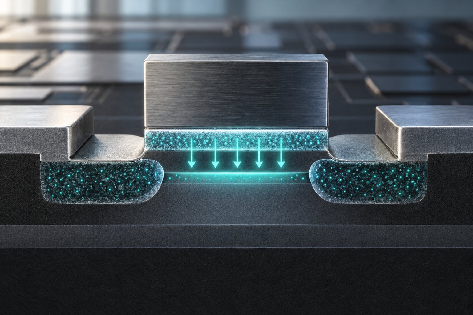
High-k metal gate technology is the gate stack used in modern CMOS transistors: a high-dielectric-constant metal oxide film (almost always hafnium oxide, HfO2) replaces the silicon dioxide insulator, and a metal electrode replaces the polysilicon gate. The dielectric cuts gate leakage, the metal removes polysilicon’s depletion effect, and together they keep transistors controllable as they shrink.
Below is the version of the explanation I wish I had when I started reading process flow decks: no unexplained symbols, the physics separated from the manufacturing, and a clear line between what high-k fixes and what the metal gate fixes.
Table of Contents
- What Is High-k Metal Gate Technology?
- How High-k Metal Gate Technology Works
- Why Conventional SiO2 and Polysilicon Gates Fell Short
- How High-k and Metal-Gate Materials Solve the Problem
- How the High-k Gate Dielectric Controls the Channel
- Why the Metal Part of the Metal Gate Matters
- High-k Metal Gate Technology in the Transistor Fabrication Flow
- What High-k Metal Gates Change in Device Performance
- Process and Design Challenges
- Frequently Asked Questions
- What does high-k mean in a metal gate?
- Why is the high-k dielectric physically thicker than silicon dioxide?
- Is a metal gate the same thing as a high-k gate dielectric?
- What is equivalent oxide thickness, or EOT?
- Does high-k metal gate technology always improve transistor speed?
- Why is hafnium oxide used for many modern CMOS high-k dielectrics?
- Conclusion
What Is High-k Metal Gate Technology?
High-k metal gate (HKMG) technology is the pair of changes that replaced the old silicon dioxide plus polysilicon gate in CMOS logic. The insulator became a material with a much higher dielectric constant, and the electrode above it became a metal rather than heavily doped polysilicon.
The name hides two separate inventions. Engineers call the dielectric a high-k material, where k is the dielectric constant. They call the electrode a metal gate. Shipping one without the other was never practical, which is why the two are almost always discussed as a single transition.
The five features that matter most:
- Lower gate leakage. A physically thicker film blocks electrons that would otherwise tunnel straight through a sub-2nm oxide.
- Higher gate capacitance. More charge stored per volt, so the gate steers the channel harder without a thinner insulator.
- A small equivalent oxide thickness. Electrical thickness keeps shrinking even though the physical film does not.
- No polysilicon depletion. A metal has no charge-depleted region to squeeze the effective oxide, so the gate reaches the channel more directly.
- Work-function metal stacks. Threshold voltage is tuned by choosing electrode materials rather than by changing doping chemistry alone.
Key takeaways: High-k means high dielectric constant, not a thick insulator. EOT, not physical thickness, is what a designer cares about. HfO2 and a metal gate are the production pairing. The combination arrived in volume logic manufacturing around 45nm in 2007 and is now universal at advanced nodes.
How High-k Metal Gate Technology Works
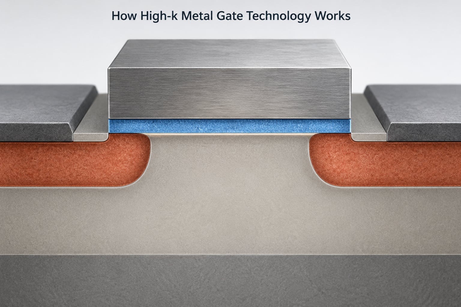
Start with a capacitor model, because that is exactly what the gate is. Two conductive plates separated by an insulator store charge when a voltage is applied across them, and the amount of charge depends on the capacitance. In a MOSFET the two plates are the gate electrode and the silicon channel, and the channel is deliberately made conductive only when you want it to conduct.
Capacitance goes up when the plate area grows or when the insulating gap shrinks. It also goes up when the insulator itself stores charge more effectively, which is what a dielectric constant describes. For a plate capacitor the capacitance scales as the dielectric constant divided by the physical thickness.
That single relationship is the whole trick. Silicon dioxide has a k value near 3.9. Hafnium oxide sits near 25, roughly six times higher. A 3.5nm film of HfO2 therefore stores about the same charge as a 0.6nm layer of SiO2 would, while physically being almost six times thicker. The insulator is doing the same electrical job through a different mechanism.
Gate depletion is the part people miss. In the old stack, when you applied a bias, the polysilicon itself became partly depleted of its carriers. That depleted region acted as extra insulation in series with the oxide, so the effective insulating distance was longer than the drawn oxide. A metal has a sea of free carriers and no depleted zone, so this series resistance disappears.
Gate length is the third lever. Because capacitance scales as k divided by thickness, you can shrink the drawn gate length while keeping enough capacitance per unit area to switch the channel. That is what allowed the physical gate length to keep shrinking alongside the channel.
Why Conventional SiO2 and Polysilicon Gates Fell Short
The classic gate oxide was grown by heating silicon in oxygen, which produced something remarkable: a silicon dioxide layer so close in atomic structure to the underlying silicon that the interface was nearly defect-free. For decades that single fact carried the whole industry.
Then the scaling targets kept shrinking. The oxide thinned with everything else, and below roughly 2nm electrons stopped being blocked by the band gap and started tunnelling through it. Direct quantum tunnelling current rises exponentially as the barrier narrows, so a small decrease in oxide thickness produced a large increase in standby leakage. Heat and battery drain followed.
The polysilicon electrode failed in a different way. Dopant concentration has a limit, so the depletion effect ate into the effective oxide and cost drive current. Sheet resistance in the gate also grew as the gate narrowed, slowing the signal reaching the channel. And below a certain gate length, the depletion region itself pushed carriers into the channel, effectively forcing the device toward depletion-mode operation with poor on-state behaviour.
There was also a work-function problem. Doped polysilicon reaches a limited effective work function, and threshold voltage targets kept moving as channel engineering and strain changed the underlying electrostatics. Designers had very little room left to tune the threshold.
| Property | SiO2 + polysilicon | HfO2 + metal gate |
|---|---|---|
| Dielectric constant | About 3.9 | About 25 for HfO2 |
| Physical dielectric thickness at same EOT | Under 2 nm | Roughly 3 to 4 nm |
| Gate leakage | Rises sharply through direct tunnelling | Several orders lower at equal EOT |
| Poly depletion | Present, costs effective oxide thickness | Eliminated, metal is a good conductor |
| Gate sheet resistance | Rises as gate narrows | Lower, so switching is faster |
| Threshold voltage tuning | Doping chemistry, limited range | Work-function metal stack selection |
| Thermal budget | Cheap, high temperature compatible | Metal limits later high-temperature steps |
How High-k and Metal-Gate Materials Solve the Problem
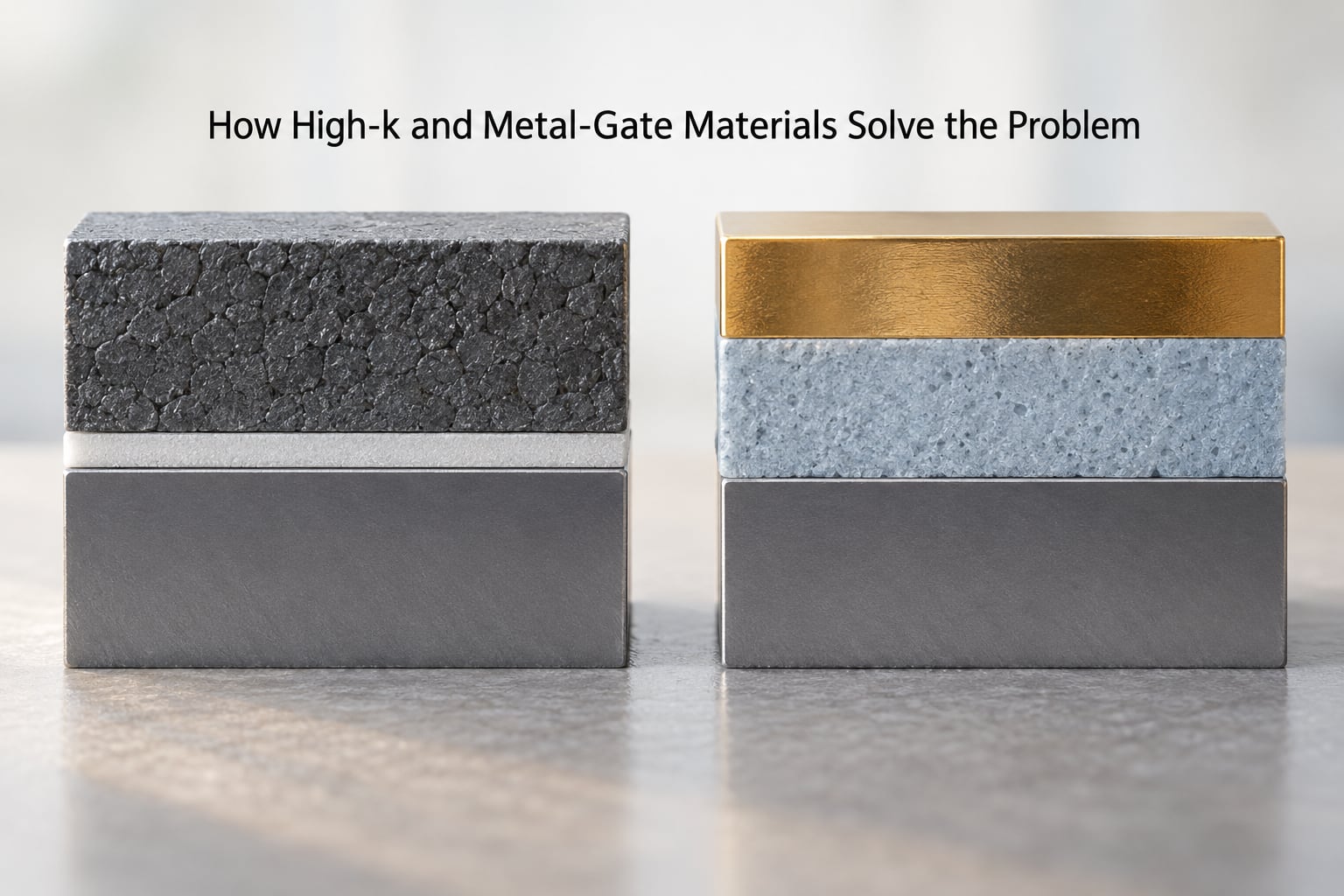
The dielectric constant is the number that decides whether a material is worth trying. Vacuum is 1, silicon dioxide is about 3.9, and the metal-oxide candidates that matter sit far higher.
| Material | Dielectric constant | Why it is or is not used at the gate |
|---|---|---|
| Air / vacuum | 1.0 | Reference value only |
| Silicon dioxide | About 3.9 | Excellent interface, but tunnels below about 2 nm |
| Silicon nitride | About 7 to 8 | Used as a blocking layer inside the gate dielectric |
| Aluminium oxide | About 8 to 10 | Lower k than the leaders, useful as a cap |
| Zirconium dioxide | About 22 to 25 | Strong candidate, less stable against silicon |
| Hafnium oxide | About 20 to 25 | Industry standard: high k, wide band gap, stable on silicon |
Hafnium oxide won for a combination of reasons rather than one headline number. Its k value is high enough to cut physical thickness. Its band gap is wide enough to block electrons by a normal barrier rather than relying on thickness alone. It forms a high-quality interface with silicon, which some earlier candidates did not. And it can be deposited in angstrom-accurate layers by atomic layer deposition, where self-limiting surface reactions cycle a precursor gas and purge step.
The metals took longer to settle. Candidates in production and development include titanium nitride, tantalum nitride, aluminium, tungsten, and, as a fallback, doped polysilicon in some flows.
| Material | Work function | Process notes |
|---|---|---|
| Titanium nitride | Mid-gap, tunable by nitrogen content | Common base layer and fill metal; etch resistance is a concern |
| Tantalum nitride | Near mid-gap, tunable by composition | Widely used as a work-function layer in production stacks |
| Aluminium | Low work function, close to the silicon band edge | Low resistance, low thermal budget, historically plasma-damaged |
| Tungsten | High work function, near the valence band | Used as a fill and contact metal; its work function suits p-type devices |
| Doped polysilicon | Limited tuning range | Retained in some flows where metal processing conflicts with the flow |
How the High-k Gate Dielectric Controls the Channel
The gate sets the threshold voltage, which is the gate-to-source voltage at which the channel starts conducting. That number is chosen to sit low enough that the transistor switches on strongly, but high enough that it stays off when the voltage is zero.
Step by step, with no bias applied, the silicon surface is lightly inverted by the built-in fields of the source and drain. Apply a positive gate bias and positive charge collects on the gate. That field repels holes and attracts electrons to the surface, thinning the depletion region and eventually forming an inversion layer of electrons a few atomic layers thick. Apply more bias and the inversion charge grows roughly in proportion to gate voltage, which is the drive current the circuit depends on.
Because the inversion layer is only a few atoms deep, the gate’s electrostatic control has to be sharp. Every extra layer of effective insulation between gate and channel weakens that control, and a weak field means the transistor needs more voltage to switch, which means more power. Keeping the equivalent oxide thickness small is therefore not just about leakage. It is about how tightly the gate can hold the channel.
Channel charge depends on the ratio of gate capacitance to the oxide capacitance the channel presents. Raising the dielectric constant raises the gate capacitance without the channel-side penalty, so the control improves. Interface traps, on the other hand, sit right at the silicon boundary and steal part of that control, which is why their density is one of the most closely watched numbers on any node.
Why the Metal Part of the Metal Gate Matters
The metal electrode arrived for three reasons, and it is worth keeping them separate because they are often blurred together.
The first is the elimination of depletion. A doped polysilicon gate depletes near the interface as bias is applied, so the effective insulating distance is larger than the drawn oxide. That lengthens the effective channel and cuts drive current. Metal does not deplete, so the drawn gate length is the real gate length.
The second is resistance. Polysilicon sheet resistance grows as the gate narrows, and the gate signal has to reach both edges of the channel quickly. Metals like aluminium and titanium nitride offer lower resistance, so the transistor switches faster at the same geometry.
The third is threshold voltage control, and this is the subtle one. A threshold voltage depends on the difference between the gate work function and the silicon work function. With polysilicon, the effective work function is pinned by how much dopant you crammed into it, and the range is narrow. With metals, you can select and stack materials to land near the conduction band edge for n-channel devices or the valence band edge for p-channel devices, which maximises drive current at a given voltage.
The complication is Fermi level pinning. Once a high-quality high-k film touches silicon, the electrical properties of the interface pin the effective work function near silicon’s intrinsic level regardless of which metal sits on top. That is why capping layers such as aluminium nitride were added between the high-k and the metal: the dipole they create shifts the barrier deliberately instead of letting the interface decide.
Work-function metals also have to survive later processing. Some lose their desired work function when exposed to high-temperature activation steps, so foundries use stacks that are robust at the thermal budget of their flow.
High-k Metal Gate Technology in the Transistor Fabrication Flow
Exact sequences differ between foundries and change with each node, but the gate-last flow has been the industry default since the early 2010s. It looks roughly like this.
- Active area and isolation. Wells, field isolation, and the source-drain regions are defined first.
- Fin or channel formation. On planar nodes the channel is the exposed silicon surface; on FinFET and gate-all-around nodes it is a shaped silicon body.
- High-k deposition. A thin silicon-rich or silicon interface layer, then hafnium oxide, deposited by atomic layer deposition for thickness control down to angstroms.
- Gate electrode deposition and patterning. Work-function metals, a barrier or fill layer, and the main conductor are laid down, then the gate is patterned.
- Gate stack clean-up. Chemical mechanical planarization removes the gate metal above the areas where source and drain will form.
- Spacer formation. A dielectric spacer isolates the gate from the source and drain extensions.
- Extensions and deep source-drain. Silicon is selectively grown or etched to form the extension regions, then heavy doped source and drain.
- Dopant activation. A thermal step, anneal, or laser anneal repairs implantation damage and places the dopants electrically.
- Silicide and contacts. Low-resistance silicide is formed on source, drain, and gate, then contacts and interlayer dielectric are added.
- Backend metallisation. Standard copper or aluminium wiring completes the chip.
Gate-last won because it keeps the high-k and metal stack from being exposed to the heavy thermal steps that follow source-drain formation, which would otherwise drive dopant diffusion in the metal and shift its work function.
| Aspect | Gate-first | Gate-last |
|---|---|---|
| When the gate stack is formed | Before source and drain | After source and drain anneal |
| Thermal budget for the metal | Must survive high-temperature activation | Added later, so the budget is gentler |
| Silicide formation | Metal must tolerate the silicide step | Simpler, metal not present during silicide |
| Work-function stability | Harder to hold the target value | Easier to hold through the anneal |
| Adoption today | Largely retired | Standard for planar and 3D nodes |
What High-k Metal Gates Change in Device Performance
Leakage is the headline. At matched equivalent oxide thickness, the tunnelling barrier through a wide-band-gap high-k film is much taller than through silicon dioxide, so gate leakage falls by several orders of magnitude. That is what keeps standby power inside the power budget as billions of transistors sit switched off.
Drive current improves because there is no depleted polysilicon layer eating into the effective oxide, and because the work-function metals land close to the silicon band edges. Current per micron of gate width goes up at a given supply voltage, which lets designers lower the voltage for the same performance.
Switching speed follows from resistance and capacitance. A lower-resistance gate and higher gate capacitance reduce the time constant, and the metal gate also reduces the capacitance seen by the interconnect above it, which helps timing on long wires.
Electrostatic control improves at short gate lengths, which reduces drain-induced barrier lowering and lets a device hold its threshold with less variation. That is a reliability argument as much as a performance one.
Density gains come indirectly. Lower leakage means lower supply voltage is viable, and lower voltage means the transistors can be packed without thermal limits becoming the constraint. No two nodes convert this into identical gains, though. Process design optimisers balance leakage, drive current, and capacitance against each other, and once a stack is chosen, later nodes are constrained by what it can do rather than by what it theoretically could.
Process and Design Challenges
Making this work in a fab is harder than the physics suggests.
- Remote-plasma deposition. Plasma-assisted ALD raises deposition rates for the gate dielectric, but stray ions can damage the silicon surface, and the dielectric must be protected from further plasma exposure.
- Chemical mechanical planarization. After the gate metal is deposited, everything above the source-drain regions has to come off cleanly without dishing the gate or scratching the channel.
- Interface traps. Defects at the high-k to silicon boundary trap charge and degrade both threshold voltage and mobility. Every generation reduces the defect density of that interface.
- Fixed charge. Charge trapped in the bulk or at interfaces shifts threshold voltage and varies across a wafer, which hurts matching between neighbouring transistors.
- Low-resistance fill. The gate has to be filled completely without voids, and the fill material must not diffuse into the dielectric during later thermal steps.
- Thermal budget. Once a low-work-function metal is in the stack, no later step may exceed its thermal stability, which constrains dopant activation and silicide formation.
- Work-function variation. Composition and thickness of the work-function layers shift across large wafers, and that variation shows up directly as threshold voltage variation.
- Reliability. Time-dependent dielectric breakdown, trap-assisted tunnelling, and resistance to temperature and bias remain the core gate-stack lifetime questions.
- Manufacturability and cost. Converting a fab to high-k metal gate is a full process requalification with new tools, new metrology, and new yield learning. The multi-billion-dollar fab investments that accompanied the transition in the late 2000s were a large part of why it took years to spread.
Beyond CMOS logic, the same materials show up elsewhere. High-k films are used as the capacitor dielectric in DRAM, and they are being studied for emerging devices including two-dimensional channel materials and stacked transistor configurations.
Frequently Asked Questions
What does high-k mean in a metal gate?
High-k means the insulator between gate and channel has a high dielectric constant, the factor that describes how effectively a material stores charge in an electric field. Hafnium oxide sits near 25 against about 3.9 for silicon dioxide. The phrase describes the dielectric only. The gate electrode on top of it is a separate, conductive metal.
Why is the high-k dielectric physically thicker than silicon dioxide?
Because capacitance scales with dielectric constant divided by thickness. A film with a much higher k value delivers the same charge at a greater physical thickness, which is exactly what a tunnelling barrier needs. The insulating distance stays large in nanometres while the electrical thickness stays thin, so electrons cannot tunnel through.
Is a metal gate the same thing as a high-k gate dielectric?
No, they are two different layers solving two different problems. The high-k dielectric sits between the gate and the channel and reduces leakage. The metal gate is the electrode above it and removes polysilicon depletion, lowers resistance, and allows threshold voltage tuning through work-function selection. They ship together because neither solves the other’s problem.
What is equivalent oxide thickness, or EOT?
EOT is the thickness of silicon dioxide that would store the same capacitance as the real gate dielectric. It is the number that matters for leakage and control, not the drawn thickness. A 3.5nm film of hafnium oxide at a k of about 25 corresponds to roughly 1.4nm of silicon dioxide, achieved with a barrier that electrons cannot tunnel through.
Does high-k metal gate technology always improve transistor speed?
Not always, and not on every node. It lowers gate resistance and removes depletion, both of which help speed, and it enables lower supply voltage. But once the stack is fixed, designers balance leakage against drive current and capacitance, and some node choices deliberately trade speed for density or power. Treat speed gains as node-specific rather than automatic.
Why is hafnium oxide used for many modern CMOS high-k dielectrics?
Hafnium oxide combines a high dielectric constant near 25 with a wide band gap, so it blocks electrons through a real barrier instead of relying on thickness. It also forms a high-quality interface with silicon and can be deposited in angstrom-accurate layers by atomic layer deposition. Earlier high-k candidates offered good k values but unstable interfaces.
Conclusion
High-k metal gate technology survives four ideas. First, the gate is a capacitor, and capacitance scales with dielectric constant over thickness. Second, equivalent oxide thickness, not drawn thickness, is what governs leakage and channel control. Third, a metal gate removes the depletion region that polysilicon created, so the drawn gate length becomes the real one. Fourth, threshold voltage is set by work-function materials chosen from a stack rather than by doping alone.
Get those four straight and the rest of the topic, from atomic layer deposition to chemical mechanical planarization to Fermi level pinning, falls into place as engineering consequence rather than mystery.