Semiconductor units of measure are the standard quantities used to express physical size and electrical behaviour across chip design, wafer fabrication, packaging and test. The short list: angstrom (Å) and nanometre (nm) for atomic and device features, micron (µm) and millimetre (mm) for wafer and die dimensions, mil and inch for package drawings, square millimetre (mm²) for die area, defects per square centimetre for fab defectivity, and ohm per square (Ω/sq), electron volt (eV) and watt per square centimetre (W/cm²) for electrical and thermal behaviour.
Getting one of these wrong is the fastest way to be wrong by a factor of a thousand. Mixing up µm with nm, or treating 12 inch as 12 mm, produces die sizes that cannot exist. It is also the key to understanding why a node called 3nm does not contain a feature that measures 3nm.
This guide walks the whole unit system the way an engineer uses it: what each unit measures, how it converts, and where the conventions quietly break.
Table of Contents
- Semiconductor Units of Measure at a Glance
- How Do Semiconductor Prefixes Work?
- What Does a Nanometer Process Node Mean?
- How Are Semiconductor Units of Measure Explained for Dimensions?
- How Do Frequency, Clock Speed, and Time Units Work?
- What Do Voltage, Current, Power, and Energy Measure?
- How Do Memory Capacity Units Differ?
- What Units Are Used for Wafers, Die, and Yield?
- Which Semiconductor Units Require Special Caution?
- Frequently Asked Questions
- What is the main unit used to describe semiconductor process nodes?
- Are a 5 nm, 7 nm, and 3 nm process physically the same size?
- Why is a 256 GB drive shown as less than 256 GB on a computer?
- Are hertz and gigahertz measures of the same thing?
- How are wafer diameters and dies per wafer measured?
- Conclusion
Semiconductor Units of Measure at a Glance
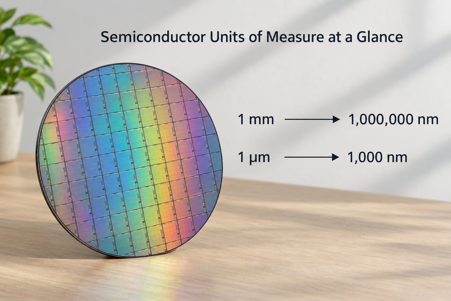
Every measurement in the industry is anchored to SI base units, but each discipline picks a different sub-unit. Process engineers work in nm and Å, packaging engineers in µm and mil, procurement in inches, and nobody outside a metrology lab works in metres.
| Quantity | Units used | Symbol | What it measures | Typical context |
|---|---|---|---|---|
| Atomic length | Angstrom, nanometre | Å, nm | Atomic spacing, gate oxide, film thickness | Interface layers, node labels, Intel 18A |
| Feature length | Nanometre, micron | nm, µm | Gate pitch, fin height, interconnect pitch | Process design rules, node comparison |
| Wafer size | Millimetre, inch | mm, in | Wafer diameter and centre-point thickness | SEMI spec sheets, purchase orders |
| Package size | Mil, inch, micron | mil, in, µm | Lead frame, die thickness, ball pitch | Assembly drawings, pad and pitch specs |
| Area | Square millimetre, square centimetre, square inch | mm², cm², in² | Die area, wafer area, surface area | Floorplanning, cost per die, defect density |
| Defect density | Defects per square centimetre | defects/cm² | Contamination rate on a surface | Particle monitoring, yield modelling |
| Voltage | Millivolt, volt | mV, V | Electric potential difference | Supply rails, I/O, core voltage domains |
| Current | Microampere, milliampere, ampere | µA, mA, A | Rate of charge flow | Leakage, short-circuit limits |
| Resistance | Ohm, ohm per square, ohm-centimetre | Ω, Ω/sq, Ω·cm | Opposition to current | Sheet resistance films, bulk resistivity |
| Power | Milliwatt, watt, watt per square centimetre | mW, W, W/cm² | Energy per second, heat per area | TDP, thermal design, power density |
| Energy | Joule, electron volt | J, eV | Work or charge energy | Switching energy, band gap, ionisation |
| Frequency | Hertz, kilohertz, megahertz, gigahertz | Hz, kHz, MHz, GHz | Cycles per second | Clock speed, refresh rate, signalling rate |
| Time | Nanosecond, picosecond | ns, ps | Elapsed duration | Access time, hold time, propagation delay |
| Memory | Bit, byte, decimal GB, binary GiB | b, B, GB, GiB | Capacity and data width | DDR parts, storage, register files |
| Throughput | Wafer starts per hour, layer count, dies per wafer | WPH, layers, dies | Counts and rates of production | Fab capacity, cost per good die |
| Ratio | Percent, parts per million | %, ppm | Fraction of a whole | Yield, defect limits, purity |
One unit sits in this table in an unusual way. Defects per square centimetre is an areal density rather than a length or an area, so you cannot convert it into nm or mm² by multiplying. It is a count spread over an area, and it behaves differently in every calculation you do with it.
How Do Semiconductor Prefixes Work?
Every unit above except a handful is an SI base unit with a decimal prefix attached. Each prefix is a power of ten, and the capitalisation matters because the scale changes in steps of a thousand.
| Prefix | Symbol | Factor | Where it shows up |
|---|---|---|---|
| Pico | p | 10^-12 | picosecond, picofarad |
| Nano | n | 10^-9 | nanometre, nanosecond |
| Micro | µ | 10^-6 | micron, microampere, microwatt |
| Milli | m | 10^-3 | millimetre, millivolt, milliampere |
| Centi | c | 10^-2 | centimetre, used in defect density |
| Deci | d | 10^-1 | decimetre, rarely used in chip work |
| (none) | — | 10^0 | metre, gram, second, volt, ampere |
| Kilo | k | 10^3 | kilohertz, kilogram |
| Mega | M | 10^6 | megahertz, megawatt |
| Giga | G | 10^9 | gigahertz, gigabit per second |
| Tera | T | 10^12 | terabit per second, terahertz |
The trap is case. A lowercase m is milli and a lowercase n is nano, while an uppercase M is mega. Read “1 mW” as a milliwatt and “1 MW” as a megawatt, and you have a thousand-fold error on a power budget.
Storage capacity breaks from this system. IEC binary prefixes add an i: KiB, MiB, GiB, TiB. Each is a power of two, not ten, and each operating system may or may not show the units the hardware label uses.
| Decimal (SI) | Bytes | Binary (IEC) | Bytes | Gap |
|---|---|---|---|---|
| 1 kB | 1,000 | 1 KiB | 1,024 | 2.4% |
| 1 MB | 1,000,000 | 1 MiB | 1,048,576 | 4.9% |
| 1 GB | 1,000,000,000 | 1 GiB | 1,073,741,824 | 7.4% |
| 1 TB | 10^12 | 1 TiB | 1,099,511,627,776 | 10.0% |
What Does a Nanometer Process Node Mean?
A nanometer process node is a generation name, not a measurement of any single feature. A 3nm node does not mean the smallest feature in the process measures 3nm. Foundries name nodes to mark a step in their roadmap, and since the mid-2000s the label has drifted away from the geometry it once tracked.
The clearest evidence is Intel 10nm, whose measured dimensions were published before launch. Its fin pitch was 34nm, fin height 53nm, minimum metal pitch 36nm, cell height 272nm and gate pitch 54nm. Not one of those numbers is 10nm.
| Node label | Architecture | Typical gate or contacted gate pitch | Typical metal pitch |
|---|---|---|---|
| 32 nm | Planar bulk | ~100 nm | ~112 nm |
| 22 nm | FinFET | ~80 nm | ~80 nm |
| 14 nm | FinFET | ~70 nm | ~64 nm |
| 10 nm | FinFET | ~54 nm | ~36 nm |
| 7 nm | FinFET / EUV | ~48 nm | ~27 nm |
| 5 nm | EUV FinFET | ~40 nm | ~21 nm |
| 3 nm | EUV FinFET | ~36 nm | ~16 nm |
| 2 nm | EUV GAAFET | ~30 nm | ~13 nm |
Two consequences follow. Node names cannot be compared across foundries, because Intel 10nm, TSMC 10nm and Samsung 10nm are three separate processes with three separate geometries. And the label has now outrun the nanometre itself, which is why Intel moved to 18A and 14A, where A stands for angstrom. An 18A label roughly corresponds to 1.8nm, but again as a name.
Practitioners on r/Semiconductors and on Electronics StackExchange tend to compare processes by transistors per square millimetre rather than by the label. That is the honest metric, and it is why density is quoted alongside every node announcement.
How Are Semiconductor Units of Measure Explained for Dimensions?
Dimensions are the easiest part of this system, because every length unit converts to every other by a single factor. The full ladder runs from angstrom to inch, and the only step that is not a clean power of ten is the inch to mil conversion.
| Unit | Symbol | In nanometres | In micrometres | In millimetres |
|---|---|---|---|---|
| Angstrom | Å | 0.1 | 0.0001 | 0.0000001 |
| Nanometre | nm | 1 | 0.001 | 0.000001 |
| Micron | µm | 1,000 | 1 | 0.001 |
| Mil | mil | 25,400 | 25.4 | 0.0254 |
| Millimetre | mm | 1,000,000 | 1,000 | 1 |
| Inch | in | 25,400,000 | 25,400 | 25.4 |
Two worked conversions cover most on-the-job arithmetic. First, a gate oxide of 1.2nm on a mature node is 12 Å, because 1nm is 10 Å. Second, a lead frame thickness quoted as 3 mils is 0.0762mm, because 1 mil is 25.4µm and 3 times that is 76.2µm.
| Physical feature | Typical size | Unit used |
|---|---|---|
| Silicon atom diameter | 0.235 | nm |
| Native oxide on silicon | 1 to 2 | nm |
| High-k gate dielectric (physical) | 1 to 3 | nm |
| Gate electrode width (advanced FinFET) | 10 to 14 | nm |
| Fin height | 30 to 60 | nm |
| Minimum metal half-pitch | 16 to 21 | nm |
| Interconnect dielectric thickness | 0.05 to 0.5 | µm |
| Backside passivation film | 1 to 3 | µm |
| Die thickness (advanced logic) | 50 to 300 | µm |
| Die thickness (thin for packaging) | 50 to 100 | µm |
Wafer supplier spec sheets quote in millimetres even though the trade discusses wafer sizes in inches, and both numbers appear on the purchase order. A 150mm wafer tolerance is usually written 150 +/- 0.2mm, which is an inch figure of about 5.9. The millimetre value is contractual because that is what the tool is calibrated against.
How Do Frequency, Clock Speed, and Time Units Work?
Frequency counts cycles per second. One hertz is a single cycle every second, one kilohertz is a thousand, one megahertz a million, and one gigahertz a billion. A clock running at 3GHz completes three billion rising edges every second.
Frequency and clock period are two ways of stating the same thing, and converting between them is one of the most common calculations in design. The period is the reciprocal: T = 1 / f.
| Frequency | Period | Same period, smaller unit |
|---|---|---|
| 1 kHz | 1 ms | 1,000 µs |
| 1 MHz | 1 µs | 1,000 ns |
| 1 GHz | 1 ns | 1,000 ps |
| 5 GHz | 0.2 ns | 200 ps |
At 2GHz the clock period is 0.5ns, so 500 picoseconds. A datasheet quoting a 200ps access time on a 1GHz part is describing roughly a fifth of one clock cycle, which is why access time and clock rate never get compared directly.
Signalling rates follow the same ladder. A 32Gbps serial link is 32 billion bits per second, while its rise and fall times are usually quoted in picoseconds.
What Do Voltage, Current, Power, and Energy Measure?
Voltage measures electric potential difference, current measures the rate of charge flow, and power measures energy consumed per second. In chip work these three get tied together constantly, because power is simply voltage multiplied by current.
| Unit | Symbol | Measures | Where it appears |
|---|---|---|---|
| Millivolt | mV | Potential difference, 0.001 V | On-chip sensing, offset references |
| Volt | V | Potential difference | Supply rails, I/O standards |
| Microampere | µA | Current flow | Standby and leakage current |
| Milliampere | mA | Current flow | Active core current draw |
| Ohm | Ω | Resistance | Contact and via resistance |
| Ohm per square | Ω/sq | Sheet resistance of a thin film | Heaters, sensors, transparent conductors |
| Ohm-centimetre | Ω·cm | Bulk resistivity of a material | Doped silicon, epitaxial layers |
| Siemens per centimetre | S/cm | Conductivity | Carrier mobility characterisation |
| Watt | W | Energy per second | Package power limits |
| Watt per square centimetre | W/cm² | Heat flux per area | Thermal design, heat spreaders |
| Joule | J | Energy | Energy per switching event |
| Electron volt | eV | Energy of one electron charge | Band gap, barrier heights, ionisation |
A worked example ties the set together. A core running at 0.8V and drawing 5A dissipates 4W, because P = V × I. Spread that over a 100mm² die and the power density works out at 4W/cm², since 100mm² is 1cm². That sits at the low end of what a modern copper lid and heat spreader can carry without a thermal design review.
Two of those rows confuse people regularly. Sheet resistance in Ω/sq is a property of a film at a stated thickness, so the number means nothing without the thickness beside it. Resistivity in Ω·cm is a bulk material property, and converting between the two requires dividing by film thickness in centimetres.
How Do Memory Capacity Units Differ?
Memory units split cleanly into decimal and binary, and the mismatch between them is the reason a formatted drive shows less than the number on the box. Vendors advertise in decimal powers of ten. Operating systems and memory tooling traditionally report in binary powers of two.
A 256GB drive holds 256,000,000,000 bytes. Formatted with a filesystem that also reserves space for its own structures, it reports roughly 238GiB, because 238 × 1,073,741,824 is about 255.5 billion bytes. Nothing was removed; two different bases were used.
The second distinction is bit versus byte, and it is the one that bites hardware engineers. A DDR part marketed as 16Gb holds 16 gigabits, which is 2 gigabytes. Register width compounds the confusion: a 32-bit bus transfers 4 bytes per clock, so a 32-bit interface running at 3GHz has a theoretical bandwidth of about 12GB/s before overhead.
| Term | Definition | Example |
|---|---|---|
| Bit (b) | One binary digit | 1 bit: on or off |
| Byte (B) | 8 bits | 1 B = 8 b |
| Kilobyte (kB) | 10^3 bytes | Storage marketing |
| Kibibyte (KiB) | 2^10 bytes | Operating system reporting |
What Units Are Used for Wafers, Die, and Yield?
Wafer-level units follow standard commercial diameters that have not changed in decades. The inch figure is nominal and rounded, which is why a 300mm wafer is called a 12 inch wafer even though 12 inches is 304.8mm.
| Nominal size | Diameter (mm) | Diameter (inch) | Typical thickness | Typical use |
|---|---|---|---|---|
| 2 inch | 50.8 | 2 | 275 µm | Discrete devices, research |
| 3 inch | 76.2 | 3 | 390 µm | Analog, sensors, power discretes |
| 4 inch | 100 | 4 | 525 µm | Legacy specialty |
| 5 inch | 125 | 5 | 600 to 700 µm | Analog, mature nodes |
| 6 inch | 150 | 6 | 675 to 700 µm | Power, RF, compound semiconductor |
| 8 inch | 200 | 8 | 775 µm | Analog, MCU, power |
| 12 inch | 300 | 12 | 775 to 800 µm | Leading-edge logic and DRAM |
Beyond diameter, SEMI-standard mechanical specifications report centre-point thickness, total thickness variation (TTV), bow, warp and edge exclusion, all in millimetres. Edge exclusion is the unusable rim of the wafer and it is typically several millimetres wide, which matters directly to the die count.
Die area is quoted in square millimetres, and dies per wafer is worked out in five steps.
- Take the wafer diameter in millimetres and subtract twice the edge exclusion to get the usable diameter.
- Subtract one step size from both die dimensions, which accounts for the scribe lane between adjacent die.
- Divide the usable diameter by die width and die height to get whole die across and down, then round each down.
- Multiply those two counts for gross die per wafer, before any defect losses.
- Apply the yield model to reach net die, or good die, per wafer.
As an illustration, a 300mm wafer with a 3mm edge exclusion has a 294mm usable diameter. With a 20mm by 20mm die and a 0.2mm scribe step, each axis fits 14 die, giving roughly 196 gross die before yield. At a 90% yield model the net count lands around 176 good die.
Defect density in defects/cm² explains where that yield comes from. Random defects scale with area, so a large die accumulates more of them, and the Poisson relationship links an areal defect density to the chance that a given die is clean. The Murphy model adds a spatial term for defects that cluster, which is why real fabs often beat a pure random-defect prediction.
Throughput completes the picture. Wafer starts per hour (WPH) measures how many wafers a tool or step processes in an hour, and layer count measures how many lithography and deposition steps the process contains. Multiply a full flow of, say, 600 steps by 100 WPH and the whole tool set is asked for 60,000 wafer starts per hour, which is the normal way fabs reason about capacity.
Which Semiconductor Units Require Special Caution?
Most unit errors in chip work trace back to one of seven habits. The first is ignoring case, where mV, mW and MV differ by factors of a thousand in opposite directions.
The second is applying SI prefixes to storage. A datasheet that says 4GB is almost always 4 × 10^9 bytes in marketing, and 4 × 1,073,741,824 bytes when a controller reports it.
The third is treating bits as bytes. Half the confusion in memory part numbers comes from this alone.
The fourth is confusing peak power with average power. A thermal design is built around sustained dissipation, not the single worst number on a datasheet.
The fifth is reading frequency as performance. Clock speed in GHz does not predict throughput, because bus width, architecture and memory latency decide that.
The sixth is comparing node labels across suppliers. Intel 10nm and TSMC 10nm are unrelated geometries, and the only fair comparison is density per square millimetre or a shipped cost and power figure.
The seventh is switching between mil and millimetre inside a single drawing. Package and lead-frame documents lean on mils; wafer and die documents lean on millimetres; the same die can appear with a thickness in mils on the assembly drawing and in micrometres on the floorplan.
Frequently Asked Questions
What is the main unit used to describe semiconductor process nodes?
The nanometre is the unit printed on node names, but it labels a generation rather than a measurement. A node announced as 3nm identifies a step in a foundry roadmap, not a feature that measures 3nm. Engineers compare processes using gate pitch, metal pitch and transistors per square millimetre instead, because those are the figures a design team can actually budget against.
Are a 5 nm, 7 nm, and 3 nm process physically the same size?
No. Each smaller label does correspond to real, smaller geometry, so the trend is genuine even though the numbers are not literal. Typical contacted gate pitches fall from roughly 40nm at 5nm to about 36nm at 3nm, while minimum metal pitch drops from about 21nm to roughly 16nm. The node name compresses several dimensions into one marketing figure.
Why is a 256 GB drive shown as less than 256 GB on a computer?
The drive holds 256,000,000,000 bytes in decimal units, and the operating system reports capacity in binary units of 1,073,741,824 bytes. Filesystem structures also consume space, so the reported figure falls to roughly 238GiB. Nothing has been removed from the drive; two different unit bases were applied to the same number of bytes.
Are hertz and gigahertz measures of the same thing?
They are the same physical quantity at different scales. Hertz counts cycles per second, and gigahertz counts a billion cycles per second, so 3GHz means three billion cycles every second. Because period is the reciprocal of frequency, a 3GHz clock has a cycle time of about 0.33 nanoseconds, or roughly 333 picoseconds.
How are wafer diameters and dies per wafer measured?
Wafer diameter and centre-point thickness are measured in millimetres with calibrated non-contact tools, and tolerances are quoted against the SEMI standard even when the commercial size is called 12 inch. Dies per wafer comes from arithmetic: subtract twice the edge exclusion from the diameter, subtract one scribe step from each die dimension, divide, round down, multiply, then apply a yield model to reach good die.
Conclusion
If you learn four families first, most semiconductor specifications stop being confusing. Those are length from angstrom to inch, area in mm², the electrical set of volts, amperes, ohms per square and watts, and frequency from hertz to gigahertz. Wafers, die counts and yield come fifth and take longest to internalise.
Whenever two specifications disagree, check four things before either number moves. Confirm the prefix and its capitalisation, confirm the symbol rather than the word, confirm whether the unit is decimal or binary, and confirm the context, since a node label is a name and not a measurement. That sequence resolves nearly every unit argument I have seen on a chip project.