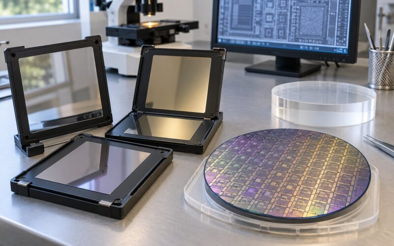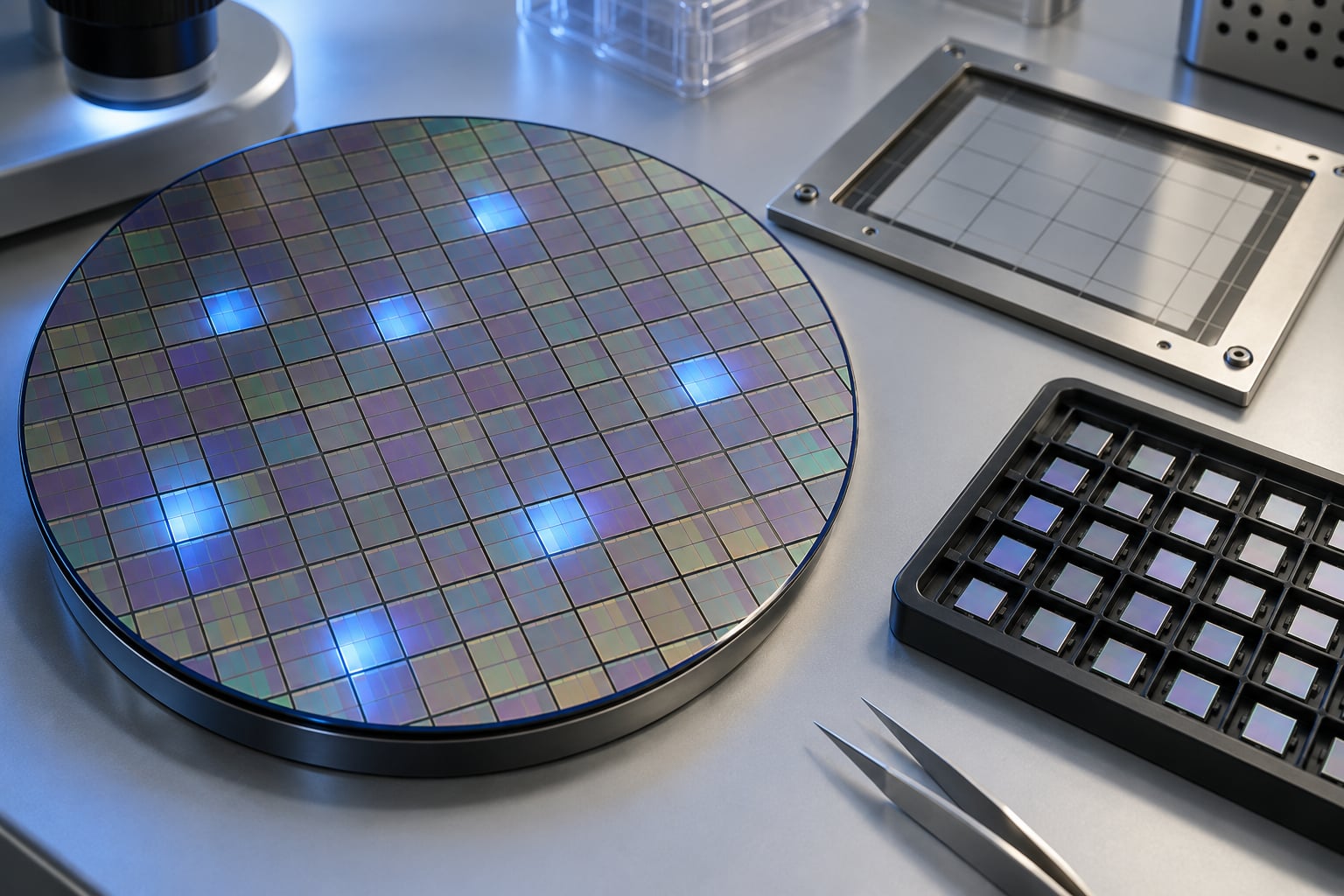
A multi-project wafer shuttle, usually shortened to MPW and also called a multi-project chip or a shuttle run, is a scheduled fabrication slot in which several unrelated chip designs are placed side by side on one wafer and share a single photomask set. Each participant pays a share of the mask and wafer cost and receives a small batch of prototype dies instead of a production lot.
That split is the whole idea. Mask tooling is the dominant fixed cost in chip development and it barely changes whether you need fifty parts or five thousand. A shuttle turns that one-off cost into a per-area charge shared across dozens of designs, which is the reason a four-person startup or a university lab can hold working silicon in its hand.
What follows is the practical version: how a shuttle is assembled, what ends up on the wafer, how the cost is worked out, what you receive at the end, and the parts of the process a shuttle genuinely does not cover.
Table of Contents
- What a Multi-Project Wafer Shuttle Is
- Why the older name multi-project chip still shows up
- Why Foundries Offer Multi-Project Wafer Shuttles
- How a Multi-Project Wafer Shuttle Works Step by Step
- Step 1: Pick a shuttle and a process
- Step 2: Get the process design kit and sign the paperwork
- Step 3: Design, close, and verify
- Step 4: Book area and submit by the freeze date
- Step 5: Placement, reticle write, and wafer processing
- Step 6: Dicing, optional probe, and delivery
- What the calendar actually looks like
- What Happens to a Project on the Wafer
- Die allocation and the scribe lane
- Pad rings and boundary rules
- Seal rings and alignment marks
- Test structures and the neighbourhood
- What a Shuttle Run Does Not Include
- How Multi-Project Wafer Shuttle Cost Is Calculated
- The per-area charge
- Minimum area seats
- The shuttle or mask fee
- Optional services
- Design-dependent factors
- What to Prepare Before Submitting a Design
- Design and verification readiness
- Process and file requirements
- Timing and ECO planning
- Pad and area budgeting
- Test and delivery planning
- Node longevity
- Multi-Project Wafer Shuttle Versus Full Production
- What to Do After the Shuttle Returns
- Probe before you cut anything
- Bring up the power rails first
- Characterise, then isolate the failure
- Package and document everything
- Decide what the shuttle proved
- Frequently Asked Questions
- Can anyone join a multi-project wafer shuttle?
- Does an MPW shuttle include packaging and testing?
- What happens if one project on the shuttle fails?
- Are the designs on a shuttle electrically isolated?
- Can I use shuttle results to order a full production run?
- Conclusion: What to Do First
What a Multi-Project Wafer Shuttle Is
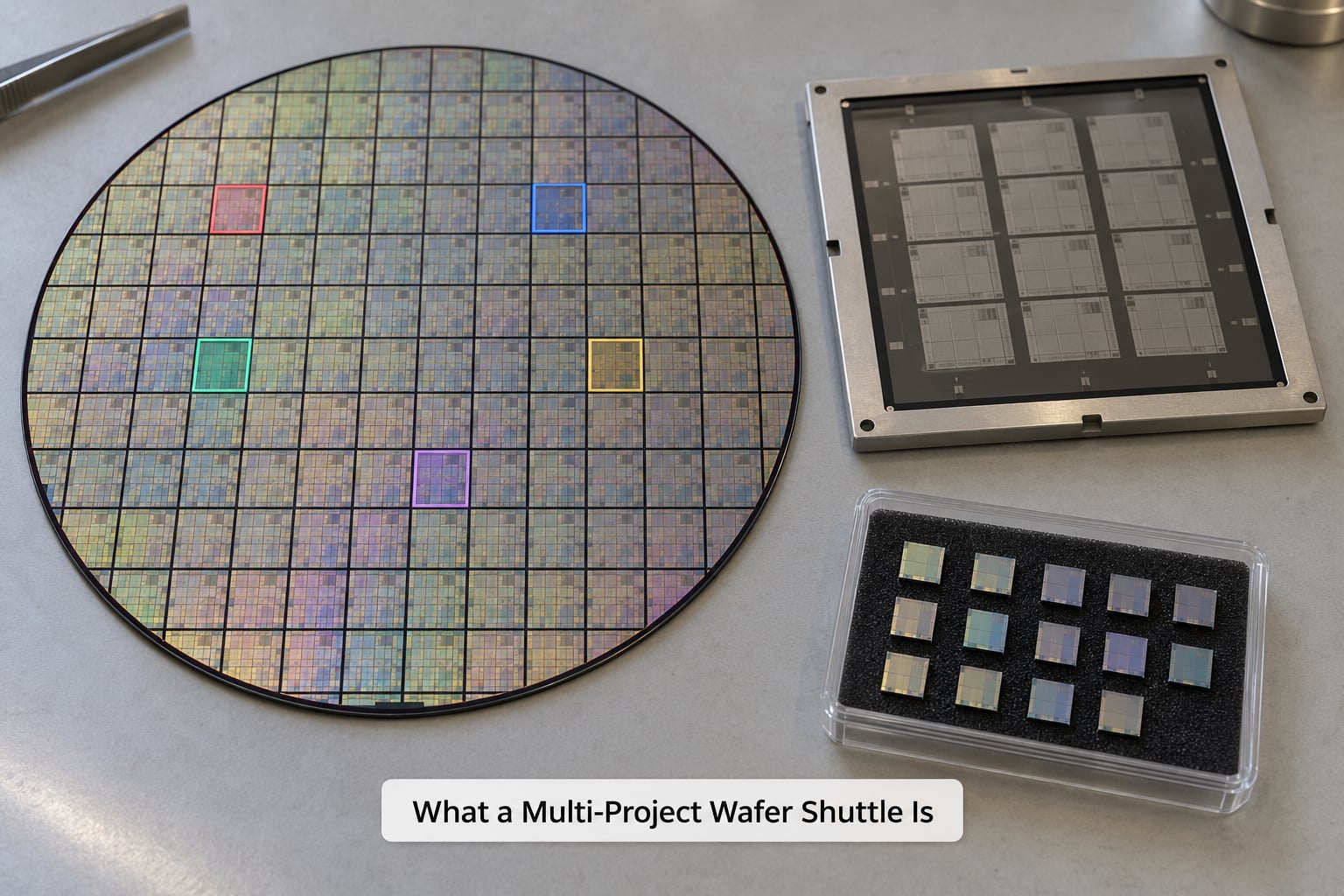
A multi-project wafer shuttle is a batch fabrication run in which a foundry or shuttle provider merges unrelated layouts from different customers into a single mask set, processes one wafer through the flow, and returns only the dies belonging to each participant.
The four things that define it:
- Shared mask set. Every accepted design is placed into the reticle field, and one mask set is built for the whole lot.
- Shared wafer processing. One wafer, or a small number of wafers, goes through deposition, lithography, etch and metallisation once.
- Area-based billing. You are charged for the die area you occupy, not for a private wafer.
- A schedule, not a purchase order. A shuttle has a submission freeze date. Miss it and you wait for the next cadence slot.
It is worth being precise about the two meanings of shuttle. One sense is the event: a dated fabrication slot with a cutoff. The other sense is the artifact: the combined reticle and the wafer built from it. People mix the two constantly, which is why shuttle deadlines get described as if they were a purchase.
The word itself comes from the shuttle payloads used in spacecraft and missiles, where several independent payloads ride one launch. Same idea, different industry.
Why the older name multi-project chip still shows up
You will also see MPC in older literature. It dates from the early days of the idea, when a shuttle was assembled from gate-level or standard-cell topologies rather than full custom layouts. MOSIS, the service that popularised the model from a 1978 MIT VLSI course, used the multi-project chip phrasing because that is what was being placed: pre-characterised blocks, not finished chips.
The name is still common in academic and government documentation. If you are reading a European research programme’s tender, MPC and MPW mean the same thing.
Why Foundries Offer Multi-Project Wafer Shuttles
Because a mask set is nearly all fixed cost. Reticle fabrication, mask writing, process setup and the engineering work to qualify a new mask set do not scale down when the wafer does. A foundry running a full production lot amortises that cost across thousands of dies. A team needing a hundred dies cannot.
Before shuttles existed, the practical choice for most small projects was to avoid custom silicon entirely: use a standard part, or a programmable device reprogrammed to do the job. That constraint shaped entire decades of product design, and it is the reason so many first-generation products are built around what was available rather than what was ideal.
Shuttles removed that constraint, and the economics still do the work today. The same fixed tooling cost is now divided among every design in the lot, so your share falls as participation rises. Programmes organised around shared shuttles also smooth out the demand curve for the foundry, giving mask shops predictable batches instead of a scatter of tiny orders.
Two knock-on effects matter. First, shuttle cadence becomes a design-planning input: a team that misses a freeze date is not losing money, it is losing a quarter. Second, because shuttle lots are the standard path to first silicon, most mature-node capacity is effectively booked through them, which is why new programs keep appearing as demand grows.
How a Multi-Project Wafer Shuttle Works Step by Step
The sequence is fixed by physics rather than preference. Masks are written once, the wafer is processed once, and nothing can be added afterwards.
Step 1: Pick a shuttle and a process
You choose an aggregator or a foundry’s own shuttle program, then choose a process and a voltage variant from what that shuttle actually offers. Some programs run several options on one shuttle; others dedicate a shuttle to a single process and layer count, which is why compatibility questions come up so often on engineering forums.
Step 2: Get the process design kit and sign the paperwork
The PDK gives you the layer definitions, the design rule deck, the device models and the standard cells for that exact revision. Sign the licensing terms, because several programs require open-source licensing of the delivered layout and others require an NDA.
Step 3: Design, close, and verify
You lay out against the design rules, run DRC and LVS, close timing, and prepare the physical verification reports the foundry will run again on receipt. This is where most shuttle schedules are won or lost, because the report must be clean against the same rule deck version.
Step 4: Book area and submit by the freeze date
Your layout goes to the shuttle provider as a GDSII file inside the booked area. The freeze is absolute. No changes are accepted after it, because placement is being finalised and the mask order is about to be placed.
Step 5: Placement, reticle write, and wafer processing
Placing several designs into one reticle field, or one wafer, is a real engineering task. The provider merges the layouts, checks for overlap and stray geometry, writes the reticle, builds the mask set, and starts the wafer through the flow. Your design sits in the queue with everyone else’s for the whole front-end cycle.
Step 6: Dicing, optional probe, and delivery
The wafer is diced along scribe lanes into individual dies. You get back your dies, and if you booked it, wafer probe results on a known-good-die list, or packaged parts in a limited quantity. Engineers still describe tape-out as mailing an envelope of layout data to the fab, and the description captures it well: it is a deadline event, not a transaction.
What the calendar actually looks like
Typical phases, on a roughly quarterly cadence:
- Design and verification window before freeze, usually several weeks to a few months depending on your team.
- Submission freeze and placement, typically one to three weeks.
- Mask set completion, commonly a few weeks once the order is placed.
- Front-end fabrication from mask order to wafer out, typically several months depending on node and slot availability.
- Back-end: dicing, optional probe, optional packaging, then delivery.
End to end, most teams describe a mature-node shuttle as several months from submission to dies in hand, and experienced engineers routinely warn that the calendar should be treated as a schedule of physical manufacturing steps, not a service-level promise.
What Happens to a Project on the Wafer
Your design is stitched into a shared surface alongside dozens of strangers. The rules that make that safe are worth knowing before you draw.
Die allocation and the scribe lane
You buy an area, and the foundry dices around it. The lane between neighbouring dies is a keep-out zone: no metal, no labels, no geometry of your own may cross it. A small design does not get rounded down to nothing, but every boundary it sits next to constrains what you can do at its edge.
Pad rings and boundary rules
Every die needs somewhere to bring power and signals in and out. That is the pad ring, and pad rules usually dictate its width and the metal it uses. Boundary rules cover the space immediately inside the pad ring, which is reserved for guard structures and routing. Together they mean your usable logic area is smaller than the area you are billed for, and the difference is not negotiable.
Seal rings and alignment marks
A seal ring between the pad ring and the die edge improves isolation and reduces leakage between neighbours. Alignment marks sit in the scribe lanes and are supplied by the foundry, which is why you do not draw your own.
Test structures and the neighbourhood
Foundries often insert process test structures, and every die may carry a small process monitor block. On advanced nodes, a design may also be placed inside a guard ring that shares with neighbours, which couples some measurements across the shuttle. For most mixed-signal and RF work, that coupling is the practical reason to plan a separated placement request early rather than assume electrical isolation.
What a Shuttle Run Does Not Include
Being clear about the edges of the service saves an expensive misunderstanding.
- Volume production. A shuttle cannot deliver thousands of parts. Even a wafer dedicated to one small design produces far fewer than a production lot.
- Leading-edge nodes. Shuttle access concentrates on mature and mid-range nodes, from the 350 nm range down to the low hundreds of nanometres. Every additional node step multiplies mask cost faster than shuttle sharing can absorb it.
- High-voltage and specialty processes. Deep trench, isolation and specialty options often need their own dedicated mask work, which pushes them out of shuttle pricing entirely.
- Full-custom analog layout. Analog and mixed-signal blocks with long routing and matching requirements need large, irregular areas that do not pack well into shared die allocation.
- Advanced packaging. Standard package options are sometimes available as an add-on. Fine-pitch, 3D, silicon photonics or chiplet packaging is a separate conversation with the packaging house.
- Production reliability qualification. A shuttle lot is an engineering lot. It tells you whether the design functions; it does not give you the yield data or qualification evidence a production release needs.
How Multi-Project Wafer Shuttle Cost Is Calculated
Shuttle pricing is not a catalogue of products. It is a formula, and once you can read the formula the offers stop looking arbitrary.
The per-area charge
The core charge is a rate per square millimetre of die area, multiplied by the area you book. That rate is what the foundry charges for wafer processing plus its share of the mask set, and it is the only number most shuttles publish clearly.
Minimum area seats
Shuttles enforce a minimum billable area, usually expressed as a standard cell or a square-millimetre seat. Small projects pay the seat price regardless of how little logic they used, which is why an 0.1 mm² design costs close to a 0.9 mm² design on a per-design basis. The floor, not your actual area, is what determines whether the shuttle suits you.
The shuttle or mask fee
On top of the area charge there is a fixed fee that covers placement, mask writing and mask set construction. It is spread across the lot, so a shuttle with many participants has a lower per-design share of that fee than a sparse one. Membership in a shuttle is therefore a real factor in the rate.
Optional services
Wafer probe, known-good-die sorting, packaging and test are quoted separately, and they can rival the area charge on a small run. Budget for them explicitly rather than assuming they are bundled.
Design-dependent factors
Process choice, layer count, voltage options, whether you need extra mask layers, the reticle field the design is placed in, and whether you ask for a separated or guarded placement all move the number. Pricing is also frequently gated behind a foundry portal or an account relationship, which is a genuine friction point: engineers report on r/chipdesign and electronics.stackexchange that published price lists are rare and estimates often have to be requested one process at a time.
What to Prepare Before Submitting a Design
Most shuttle disappointments are preparation failures, not manufacturing failures. Before the freeze date, have these settled.
Design and verification readiness
A verified schematic matched to layout, a layout clean against the exact design rule deck version you are submitting under, and a run of layout versus schematic with no unexplained nets. Verify against the foundry’s deck, not the one installed in your tool by default.
Process and file requirements
Confirm the process option, voltage variant and any required device options. Produce the layout as GDSII with the correct layer mapping for that PDK, plus the reports the foundry requires. IP blocks carry their own licence terms and foundry qualification, so check that before submission, not after.
Timing and ECO planning
Assume there will be no silicon-only fix after freeze. Do your timing closure, your clock domain crossing checks and your hold fixing before the date, and keep a metal-only change plan in case a hold violation shows up at the foundry. Experienced teams treat the freeze as an engineering milestone, not a calendar notification.
Pad and area budgeting
Include the pad ring, boundary rules and any guard structures in your area estimate. Book a little more than your logic needs. Under-booking is the single most common reason a design does not fit the shuttle slot it was quoted for.
Test and delivery planning
Decide before you submit whether you want bare dies, wafer probe results, or packaged parts. Each choice changes the quote and the delivery date, and rearranging it after the wafer is out usually means going back to the queue.
Node longevity
Check that the process will still be a sensible choice when your product ships, not just when your design is done. A two-year product built on a node already heading toward retirement creates a sourcing problem no shuttle pricing can solve.
Multi-Project Wafer Shuttle Versus Full Production
The comparison table below is the decision most teams actually need to make. If you already know your volume and your node, the right column is usually obvious.
| Consideration | Multi-project wafer shuttle | Full production run |
|---|---|---|
| Purpose | Prove the design works before committing tooling | Ship a product in volume |
| Mask strategy | One mask set shared by every design in the lot | Dedicated mask set for your design alone |
| Who absorbs mask cost | Split across all participants | Borne entirely by your project |
| What you receive | Dozens of good dies, optionally packaged in small numbers | Production quantities of qualified parts |
| Scheduling | Fixed freeze dates; miss one and you wait a full cycle | Negotiated program start, often with a longer first pass |
| Node access | Mostly mature to mid-range nodes with published shuttle options | Any node the foundry sells, including leading edge |
| Layout freedom | Area allocation and boundary rules restrict edges and long routing | Full control of die shape and internal layout |
| Main risk | Too few dies to characterise, and nothing is fully known until the wafer returns | High upfront spend before the first part exists |
| Typical path | Then a dedicated mask set or production agreement | Only after the design is proven |
The pragmatic sequence is shuttle first, dedicated mask set second. If a design proves itself, the shuttle investment has told you whether the architecture, the layout rules and the yield assumptions are real, which is exactly what you need before signing off a production mask order.
What to Do After the Shuttle Returns
The dies arriving is the midpoint, not the finish. Most projects that waste a shuttle waste it here.
Probe before you cut anything
If you booked wafer probe, work from the known-good-die list. If you did not, budget for probing as soon as the parts arrive; it tells you how many good dies you actually have and prevents you from soldering a board around a bad part.
Bring up the power rails first
Check supply currents against simulation before anything else. A current that is wildly off usually points to a short, a missing connection or a power grid problem, and it is much easier to diagnose before you spend a week chasing logic failures.
Characterise, then isolate the failure
Bring up interfaces and then functional blocks, in the order that lets each result narrow the search. When a block fails, do failure analysis early: probe the boundary, then go to emission microscopy or optical fault injection. Metal-only changes are sometimes possible on a shuttle die, but only in limited ways, and only if you have not destructively analysed the part.
Package and document everything
Package the parts you keep, and write down the lot, shuttle, wafer position and die coordinates alongside your test data. That record is what makes your next tape-out comparison possible and what a customer or reviewer will ask for if the design ever goes further.
Decide what the shuttle proved
Ask three questions. Does the design meet its specification? Which blocks need redesign? Is the process and area assumption still sound at production volume? If the answers are good, move to a dedicated mask set or a production agreement with the same foundry so you inherit the qualification already done. If the design is close but not ready, a second shuttle run is a normal and inexpensive step.
Frequently Asked Questions
Can anyone join a multi-project wafer shuttle?
Mostly yes. Commercial shuttles accept any company or individual who signs the foundry’s terms and can pay the area charge, though some require an account or a signed NDA. Open programs are stricter: MOSIS and Europractice route through academic or national membership, and programs built around open-source hardware require you to publish your design under an open licence. Check the eligibility rules of the specific shuttle before you start your layout.
Does an MPW shuttle include packaging and testing?
Usually not by default. A standard shuttle delivers diced dies, and probe, known-good-die sorting, packaging and test are quoted as separate services. Some aggregators and foundries bundle a small number of packaged samples with a shuttle order, which is convenient for bringing a design up on a board, but the quantities are limited and the package options are basic. Decide what you need to receive before you submit, because changing it later means rejoining the queue.
What happens if one project on the shuttle fails?
Nothing dramatic, and that is the point of the model. Each participant receives only the dies from their own block, so a neighbouring design that is electrically broken or simply unused does not affect your parts. The consequences are indirect: a very badly behaved design can disturb shared supplies or test structures, and a placement request for separated or guarded space may be worth making if your measurements are sensitive. The real lesson is to keep backups, because the next shuttle date is months away.
Are the designs on a shuttle electrically isolated?
Partly. Separate die areas on the wafer are physically distinct and generally well isolated, and foundry seal rings reduce leakage between neighbours. Within the shuttle reticle there can still be coupling: shared test structures, guard structures and supply references are common, especially on smaller nodes. If you are doing sensitive mixed-signal, RF or low-noise measurement, ask the provider what placement options exist and request separation or a dedicated guard ring early, while there is still time to honour it.
Can I use shuttle results to order a full production run?
Yes, in the sense that shuttle results tell you whether the design works and roughly how it behaves in silicon, which is what a production order depends on. You still need a separate path for the parts themselves: shuttle quantities are engineering samples, and volume supply means a dedicated mask set or a production agreement with the foundry. The shuttle’s real contribution is de-risking the decision, so you are ordering production silicon with evidence rather than a hope.
Conclusion: What to Do First
Start by picking the shuttle, not the circuit. The process options, area floors, deadlines and delivery format available on a given shuttle constrain your design far more than the reverse, and a layout drawn against the wrong deck or the wrong area budget is a lost freeze date.
Then book more area than your logic needs, run DRC and LVS against the exact rule deck you will submit under, and treat the freeze date as a hard engineering milestone. A multi-project wafer shuttle is a genuinely good way to get first silicon, but only if what you hand over at submission is something you would defend as finished.