Interconnect scaling challenges are the physical and economic problems that appear as the wires and vias connecting billions of transistors must shrink faster than the transistors themselves. Copper lines get more resistive, dielectric capacitance barely improves, and a barrier stack that is invisible at 14 nm swallows a large share of every cross-section by the time you reach the smallest nodes. On top of that sit patterning cost, IR drop, and reliability limits that most public explainers treat as footnotes.
Transistors scaled cleanly for decades, so the wiring quietly became the bottleneck. If you are a process, physical-design or integration engineer, understanding why the wires fell behind matters more than any single node name, because the fixes available to you are different from the fixes available to the gate stack.
This guide covers interconnect scaling challenges explained in order: the physics first, then the process and material choices, then the things a designer can actually change before tapeout.
Table of Contents
- What is interconnect scaling?
- Why do interconnect scaling challenges happen?
- How does interconnect scaling affect resistance and delay?
- Why do capacitance and signal integrity become harder to control?
- What are the main interconnect scaling challenges?
- Physical and geometric challenges
- Electrical challenges
- Manufacturing and patterning challenges
- Materials challenges
- Reliability challenges
- Design and architecture challenges
- How the challenges interact
- Which process and material choices help?
- How do designers reduce interconnect problems?
- How are interconnect effects verified?
- Frequently Asked Questions
- What are the main interconnect scaling challenges?
- Why does copper resistivity increase as interconnects get smaller?
- What is RC delay in semiconductor interconnects?
- What is the difference between interconnect pitch and process node?
- Do more metal layers solve interconnect scaling problems?
- How do designers model coupling capacitance?
- Conclusion
What is interconnect scaling?
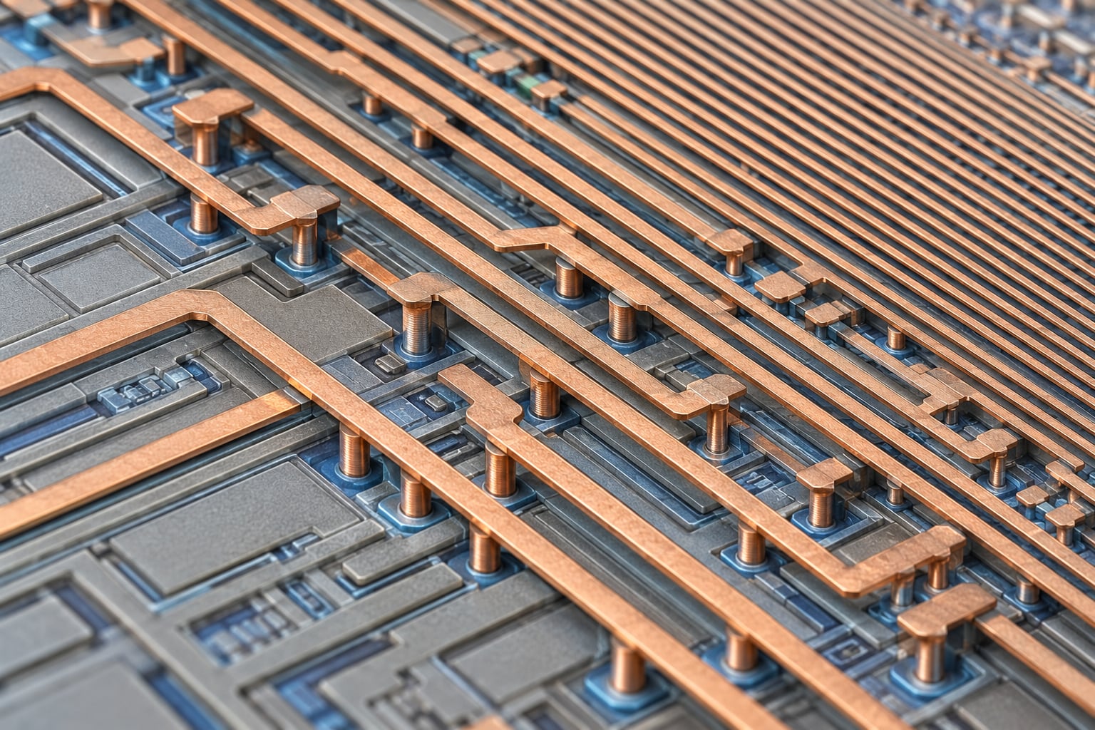
Interconnect is everything on a chip that carries a signal, a clock, or a supply between two points: horizontal metal lines, vertical vias that stitch one level to the next, and the plug that joins a via to the transistor below. No transistor does anything useful alone; the interconnect is what turns a sea of devices into a circuit.
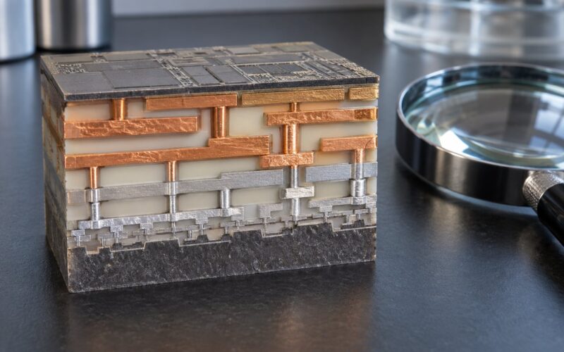
The stack is usually split into three regions. The FEOL is the front end of line, where the transistors are built. The MOL is the middle of line, holding the local contacts that reach the gates and source or drain. The BEOL is the back end of line, the thick upper metal stack that runs signals across the die and feeds power into the logic below.
Two numbers describe how tight that stack has become. The smallest line width is the width of the narrowest copper wire. The interconnect pitch is the repeating centre-to-centre spacing of a line-and-via pair, and it is the more honest metric, because a pitch encodes width, spacing and via size in one number.
Interconnect scaling means shrinking that pitch, adding levels, and keeping the electrical behavior good enough that the logic still closes timing and holds its power budget. The last part is where it gets hard.
Why do interconnect scaling challenges happen?
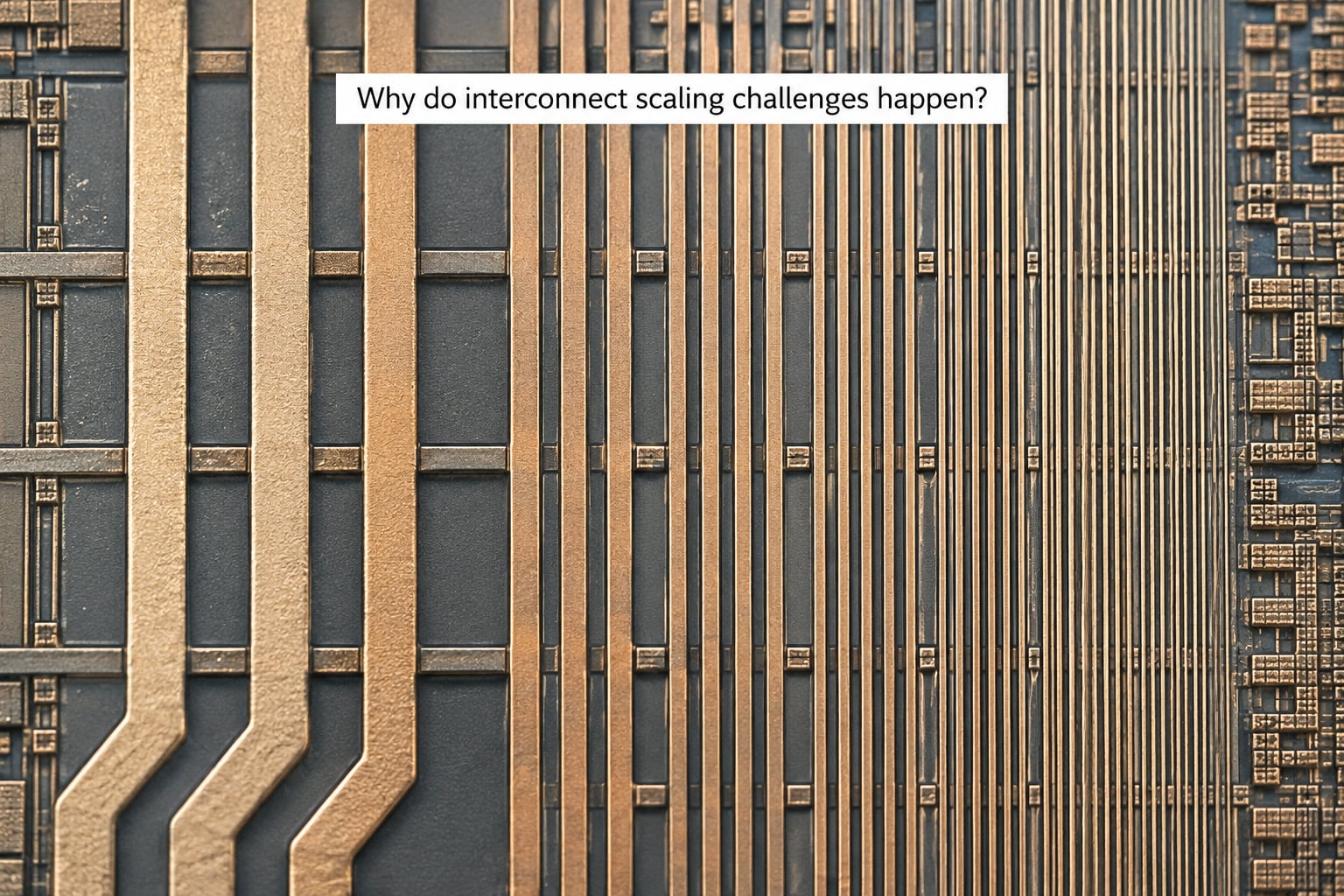
Three things happen at once when pitch shrinks, and each one is a problem on its own. First, the cross-sectional area of a wire falls, and since resistance grows as area falls, every micron of a critical net gets harder to drive. Second, the distance to a neighboring wire keeps shrinking, so coupling capacitance rises faster than the ground reference improves. Third, the number of levels keeps climbing, because designers need the extra wiring to route around each other.
Aspect ratio goes the wrong way too. A narrow line with a deep via underneath it is hard to fill, hard to clean, and hard to keep open. Vendors and foundries describe the condition as the process window narrowing: the same deposition or etch step that comfortably filled a 40 nm trench will choke on an 18 nm one.
At the same time, the switching targets keep moving. Faster transistors at lower voltage produce smaller and noisier signals, so a marginal wire that was acceptable two nodes ago now fails signal integrity checks.
Line-edge roughness matters here too. Photolithography does not produce a perfectly straight edge, and the statistical worst case of a rough edge on a narrow wire is worse than the average, which is exactly what timing analysis cares about.
The result is a stack that keeps adding levels of thinner, narrower, more expensive metal. One vendor assessment of leading-edge logic counts 18 or more metal levels, smallest wires around 13 nm, and more than 60 miles of wiring on a single die. That is not a design choice anyone enjoys; it is what the resistance and capacitance budget forced.
How does interconnect scaling affect resistance and delay?
Interconnect scaling challenges show up first as delay and power, because resistance, capacitance and the drive current of the driving gate all feed the same number. The classic expression is a distributed RC line: delay grows with the product of total wire resistance and total wire capacitance, scaled by the driver strength. Unlike transistor delay, which improves when you shrink things, wire delay gets worse as you shrink things.
Copper is the reason people expect wires to scale at all. When IBM moved from aluminum to copper in its 1998 PowerPC parts, line resistance fell roughly 40 percent with about a 15 percent speed gain. The catch is that bulk copper resistivity is a fixed material property, and once the wire is only a few tens of nanometres wide, the electrons stop behaving like a bulk fluid.
Two scattering mechanisms take over. Grain boundary scattering comes from imperfect crystal orientation at the boundaries between grains in the copper film, and it is the one grain engineering and seeding processes target. Surface scattering comes from electrons bouncing off the sidewalls of the wire, and it grows sharply as the width approaches the electron mean free path. Work reported from Samsung’s Advanced Logic Lab indicates surface and confinement effects, not grain boundaries, dominate copper resistivity at small dimensions, which is a discouraging result: the lever that engineers spent decades pulling on is no longer the big one.
The second delay term is via resistance, and it degrades faster than line resistance. A via is a short, wide contact surrounded by liner on the sidewalls and bottom, so a larger fraction of its current flows near high-resistance interfaces and thinner material. Figures published in industry analysis put via resistance rising by as much as an order of magnitude at the smallest nodes, and a TaN or Ta barrier interface with the copper fill is called out as the largest single contributor.
| Connection change | Effect on resistance | Effect on delay and power | Where it is used |
|---|---|---|---|
| Wider line | Lower, proportionally | Lower RC delay, higher routing density lost | Short, critical nets near the device |
| Thinner line | Higher, and the increase accelerates | Higher RC delay and higher IR drop | Long nets in the upper stack |
| Shorter run | Lower, close to linear | Lower delay, but harder to find space | Local routing between neighbouring blocks |
| Lower-resistivity metal or thinner liner | Lower, often by 20-30 percent | Lower delay at the same geometry | Bottom few levels, via stacks, power rails |
| Higher-resistance upper metal | Higher | Little delay impact because the wire is long and slow-switching | Top one or two levels, block-to-block routes |
Delay share moves in one direction over time. Data cited from Georgia Tech tracks the interconnect contribution to total delay climbing from about 7.6 percent between the 45 nm and 22 nm generations, to 21.8 percent between 22 nm and 11 nm, to roughly 48 percent between 11 nm and 7 nm, with industry analysis attributing more than 75 percent of total RC delay to interconnect at the leading edge.
Power follows the same physics. Roughly a third of total device power is attributed to interconnects in leading-edge process figures, because charging a wire’s capacitance every cycle costs energy whether or not the logic needs the data.
Why do capacitance and signal integrity become harder to control?
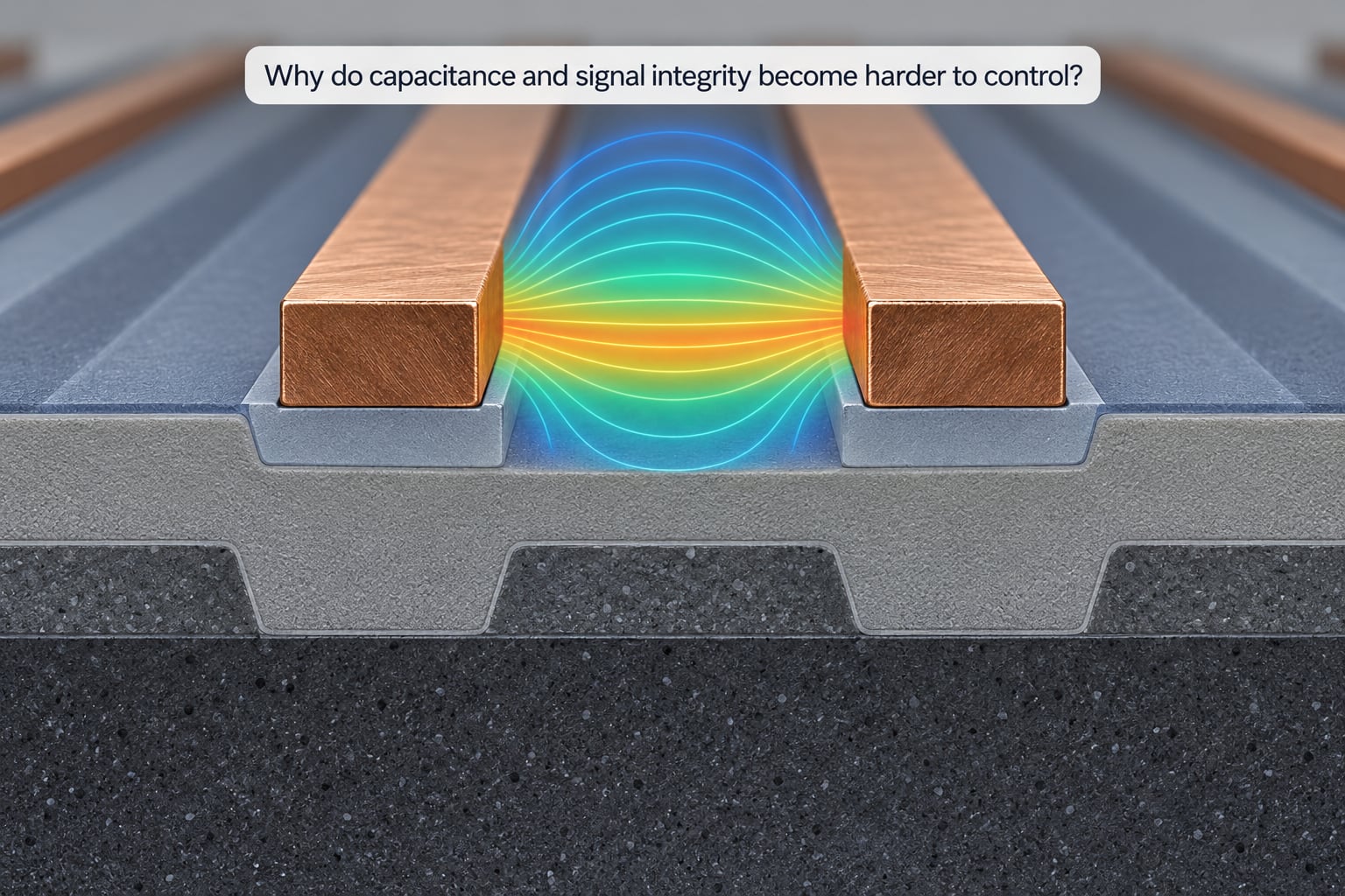
Capacitance splits into two parts, and they behave differently. Lateral capacitance is the coupling to the neighbors on the same level. Fringing capacitance is the field reaching past the wire into whatever sits above and below, which is usually the low-k dielectric but can be the neighboring metal level’s sidewall.
As pitch shrinks, lateral coupling rises because the separation falls, and the coupling coefficient climbs because the two wires look less like a capacitor and more like two plates. On a wide-pitch net the far neighbor is a rounding term. On a narrow-pitch net it is a first-order term, and the aggressor switching pulls the victim voltage directly.
What that produces in analysis is crosstalk: delay that appears on a quiet net because a neighbor moved, noise injected on a held signal, and a glitch large enough to flip a latch. Because the coupling is a function of exact geometry and exact neighbour placement, small routing differences produce timing results that differ by more than the signoff margin. This is the practical reason interconnect scaling challenges are a design problem and not only a process problem.
Aggressor and victim identification is now a routing-time task. Fixing it after the fact means respacing lines, inserting shielding, or changing layers, and all three cost area that a placed-and-routed block no longer has.
What are the main interconnect scaling challenges?
Here are the interconnect scaling challenges explained by the kind of engineering that owns each one. The categories are separate only for convenience; at the tapeout stage they all argue with each other.
Physical and geometric challenges
Pitch, aspect ratio, line-edge roughness and the fill of a via stack. At the smallest dimensions, a via that is nominally 20 nm wide has a bottom and sidewalls covered in liner and seed, so the copper that carries current is a narrow column in the middle. The remaining gap must be filled without voids that later become reliability defects.
Electrical challenges
Rising line and via resistance, coupling capacitance, crosstalk, IR drop in the power grid, and a shrinking noise margin as supply voltage falls. The power side deserves attention on its own: moving current through a resistive network costs voltage, and a cell that sees less voltage than nominal is slower than the timing library promised.
Manufacturing and patterning challenges
Wires at these dimensions come from multi-patterning with 193 nm immersion lithography or from EUV, and each extra pattern costs mask count, cycle time and yield. On the deposition side, electroplating copper and filling narrow gaps reliably is a narrow process window, and switching to a new liner metal changes the chemistry, the adhesion behaviour and the clean steps all at once.
Materials challenges
Copper is at the limit of what it can do. Low-k dielectrics have plateaued around a dielectric constant of 2.4 to 2.5 because the porosity that lowers k also destroys mechanical strength, and time-dependent dielectric breakdown gets worse as the material gets weaker. The barrier and liner stack eats an increasing share of line volume, so a nominally improved copper line can still get worse in resistance.
Reliability challenges
Electromigration moves copper atoms along the current direction until voids form and lines open. Time-dependent dielectric breakdown weakens the dielectric until it conducts. Copper is also prone to the phenomenon vendors call copper reflow, where the metal migrates during thermal cycles and can short to an adjacent line. Low-k and thin liners both make this worse, which is why new materials ship with a reliability qualification plan attached.
Design and architecture challenges
When wires set the critical path, a design flow built around gate-level optimization hits diminishing returns. Physical designers end up managing a coupled electrical, thermal and physical optimization, and the changes that help, such as promoting a net to a faster layer or buffering a long route, trade area for delay. This is the design-technology co-optimization problem, and it is where EDA vendors have concentrated their effort as of 2026.
How the challenges interact
The interaction is the real difficulty. Thinning a liner to reduce resistance reduces the barrier that keeps copper from diffusing, which costs reliability margin. Adding a low-k dielectric to cut capacitance makes the stack mechanically fragile, which raises the risk of crack-driven failures and forces more conservative mechanical design rules. Using an upper metal for a long critical net cuts delay but increases coupling into its neighbours, so an unrelated net now fails. Every fix moves a problem one layer down, and the engineer who does not model all of them at once gets a surprise at signoff or, worse, in the field.
Which process and material choices help?
| Option | Where it is used | What it buys | What it costs |
|---|---|---|---|
| Copper with TaN or Ta barrier | Established nodes, most levels | Low bulk resistivity, mature fill and CMP | High resistivity liner, growing share of line volume |
| Copper with cobalt liner | Bottom contact and via levels, single-digit nodes | Thinner liner than TaN, lower via resistance, lower IR drop | Higher film resistivity, adds a cap step and new adhesion behaviour |
| Ruthenium liner with copper fill | Narrowest lines, some via levels | Thin liner, better electromigration margin, easier gap fill | Expensive metal, CMP and contamination controls are harder |
| Ruthenium lines | Finest signal and local power levels | No thick barrier needed, low via resistance | Higher resistivity than bulk copper, new integration and reliability work |
| Ruthenium-cobalt binary liner | Leading-edge copper lines | Thinner liner than either metal alone, so a real copper cross-section gain | Two-metal system, tighter process control, supply and cost questions |
| Low-k dielectric and air gaps | All levels, air gaps at selected levels | Lower dielectric constant, lower lateral and fringing capacitance | Mechanical weakness, higher breakdown risk, extra cost; Intel reported roughly a 17 percent capacitance gain at two metal levels in its 14 nm process |
| More metal levels | Every node | Short top-level routes, smaller coupling on long nets | Cost, wafer area, thermal path, CMP steps, more vias to fail |
One test chip result is worth repeating because it sets a realistic expectation for how much any of this buys you. Applied Materials has reported a ruthenium-cobalt liner on a 2 nm-class test wafer cutting liner thickness by about a third, to roughly 20 angstroms, reducing resistance by up to 25 percent, and delivering about a 2.5 percent performance gain on the measured die. Modest, real, and worth taking seriously, because it came from a working integrated flow rather than a single film.
Below the bottom contacts, the answer has been architectural. A buried power rail moves the power network out from under the signal wires, and a backside power delivery network moves it to the far side of the wafer entirely, freeing frontside routing area. A buried power rail with backside delivery has been reported to improve voltage loss by about seven times and support 20 to 33 percent cell area scaling, which matters because the power wires were taking area that logic needed. The tradeoff is that backside delivery requires wafer thinning, backside alignment and alignment accuracy that is unforgiving.
And the other honest answer is to stop expecting planar scaling to carry everything. Chiplets, 2.5D and 3D stacking, and eventually optical links move the long-haul distance off the die, so the hardest wires travel a few microns instead of a few hundred. That does not remove the RC problem; it partitions it, and partitioning has been the strategy for every node since 1998.
How do designers reduce interconnect problems?
These are design-side levers. They do not change the process, and none of them is a substitute for a process that already has a workable resistance and capacitance budget, but together they recover a meaningful slice of the loss.
- Identify critical nets first. Run extraction and a criticality analysis before touching anything. The top few percent of nets usually hold most of the delay, and effort spent on the median net is wasted.
- Size wires by role. A clock or a high-fanout net does not tolerate the same resistance as a low-activity control signal, so give the critical ones width and the quiet ones space. Track the cost in density rather than pretending it is free.
- Assign layers deliberately. Put long, timing-critical routes on fast upper metals and short local connections on the dense lower levels. Vertical wire usage should be planned, not defaulted.
- Shield when coupling is the problem. A grounded or power line between an aggressor and a victim is the most direct fix, and it costs routing resources, so decide it early rather than after a crosstalk report.
- Buffer long routes. Splitting a long net with repeaters divides both resistance and capacitance, at the cost of area, power and a new path for the tool to time.
- Use useful skew deliberately. Adjusting clock arrival on non-critical paths gives a timing-critical net more budget without moving any logic. Done badly it converts slack into a recovery problem, so it belongs in the same flow as the rest of timing.
- Place and route with coupling in mind. Spacing rules tuned for the extracted aggressor list beat post-route fixes, because by the time a net fails, the space is gone.
- Design for manufacturability. Keep the design inside the process window with margin on via aspect ratio, spacing and density, because a design that only works at nominal etch uniformity is a design that loses yield across the wafer.
One caveat: these levers get less effective as wires get shorter relative to the gate delay of the driving cell. At some point the net is so short that buffering costs more than the wire ever did, and the honest answer is that the wire needs a better process, not a better route.
How are interconnect effects verified?
Verification happens in a loop, and each stage catches a different class of mistake. Parasitic extraction turns the layout into resistance and capacitance values, either with a fast rule-based tool early on or an accurate field solver near the end. Rules-based extraction is optimistic on coupling, which is exactly the term that matters most at tight pitch, so the accurate run is not optional before tapeout.
Static timing analysis then works on those parasitics, with corner and mode coverage. A net that passes at the nominal corner and fails at the slow corner with coupling is a net that will return from the lab. Signal integrity checks run on the extracted network to find crosstalk delay and glitch risk, and the noise analysis pass reports the margin left for aggressors. An aggressor list is the input to all of it, so getting that list right is where the accuracy is won or lost.
Electromagnetic analysis comes in when a net is long, when a via structure is unusual, or when the extracted values disagree with something. Full-wave solvers are expensive, so they are used on a sample: the vias, the wide power straps, any resonant structure, and the nets a designer already flagged.
The final loop is correlation against silicon. Pre-layout estimates are systematically wrong in known directions, because a designer must assume a fill density, a via array density and a sidewall profile. Comparing on-chip resistance measurements and measured stage delay against the extracted values turns the assumptions into constants, and that database is what makes the next node’s estimates trustworthy. Teams that skip it tend to re-discover the same correction every generation.
Reliability verification runs alongside: electromigration at current density, time-dependent dielectric breakdown on the dielectric, and thermal cycling for copper reflow. Each new liner or dielectric arrives with its own qualification criteria, because cobalt and ruthenium do not fail the same way tantalum did, and the pass criteria have to be re-derived rather than inherited.
Frequently Asked Questions
What are the main interconnect scaling challenges?
The core ones are rising line and via resistance in copper, coupling capacitance and crosstalk between tightly spaced wires, the barrier and liner consuming a growing share of each line, capacitance that low-k dielectrics can no longer reduce, IR drop in the power grid, and the cost and yield of patterning and filling them. On top of those sit electromigration, time-dependent dielectric breakdown and copper reflow reliability risks, plus the design-flow problem of critical paths that no longer sit in the gates.
Why does copper resistivity increase as interconnects get smaller?
Two effects take over. Grain boundary scattering comes from imperfect crystal orientation in the copper film, and surface scattering comes from electrons bouncing off the wire sidewalls as the width approaches the electron mean free path. Industry work from Samsung’s Advanced Logic Lab indicates surface and confinement effects dominate at small dimensions, so grain engineering stops being an effective lever exactly when it is most needed.
What is RC delay in semiconductor interconnects?
RC delay is the propagation delay of a signal through a wire, governed by the product of the line’s resistance and its capacitance, scaled by the strength of the driving gate. Unlike transistor delay, it worsens as geometry shrinks, because resistance rises as cross-section falls while capacitance stays high. Industry analysis attributes more than 75 percent of total RC delay at the leading edge to interconnect.
What is the difference between interconnect pitch and process node?
Process node is a marketing label for a generation of transistors. Interconnect pitch is a physical measurement: the repeating centre-to-centre spacing of a line-and-via pair, which encodes line width, spacing and via size in one number. Because node names no longer map to a fixed physical dimension, foundries and equipment vendors increasingly benchmark interconnect progress by pitch instead.
Do more metal layers solve interconnect scaling problems?
They relieve congestion but do not fix the physics. Extra levels give long critical routes a short, fast path and cut coupling on crowded nets, but each level adds via resistance, cost, CMP steps, area and thermal path. Leading-edge logic already carries 18 or more metal levels, and adding more layers has not reversed the trend of interconnects consuming a growing share of delay.
How do designers model coupling capacitance?
Extraction tools compute coupling capacitance from the actual layout geometry, then identify aggressor and victim nets based on switching activity and timing. Timing analysis uses those pairs to add crosstalk delay and check noise margin against the switching victim. The result depends heavily on correct aggressor identification, which is why tools differ in how much margin they hold back for nets with uncertain activity.
Conclusion
The interconnect scaling challenges explained here all trace back to one trade: resistance and capacitance both have to fall while every dimension shrinks. Start by finding out which nets actually set your critical path, then model their resistance and coupling accurately instead of trusting the fast extraction. Choose layers and materials knowing the resistance budget, not the node name, and keep the design inside the process window with margin. Validate timing, signal integrity and reliability before tapeout, then feed your measured silicon back into the extraction assumptions so the next node starts from better numbers.