JTAG basics for hardware debugging come down to four wires, a small state machine inside your chip, and a probe that lets you halt a processor, read its memory and load a bitstream while the board is running. It is the interface almost every FPGA, microcontroller and SoC exposes for exactly that job, defined by the IEEE 1149.1 standard and named after the Joint Test Action Group that wrote it.
The awkward part for newcomers is that the standard describes a test and manufacturing interface, not a debugger, yet almost every board you own uses those same four pins for real debugging. Once you see how the two jobs share the hardware, the wiring stops being mysterious.
Table of Contents
- What Is JTAG and Why Does It Matter for Hardware Debugging?
- JTAG Basics for Hardware Debugging: The Four Signal Lines
- How the JTAG TAP Controller Works
- What Is Boundary Scan and When Should You Use It?
- JTAG debugging versus boundary scan
- JTAG Basics for Common Hardware Debugging Tasks
- How to Troubleshoot Common JTAG Problems
- What JTAG Tools and Adapter Features Do You Need?
- JTAG versus SWD versus UART debugging
- Frequently Asked Questions
- What are the basic principles of JTAG debugging?
- What is JTAG debugging used for?
- What is the difference between JTAG and SWD?
- Is J-Link the same as JTAG?
- Why will my JTAG probe not detect the target?
- Does a successful JTAG connection prove the board is correct?
- Conclusion: Start With a Simple JTAG Chain Check
What Is JTAG and Why Does It Matter for Hardware Debugging?
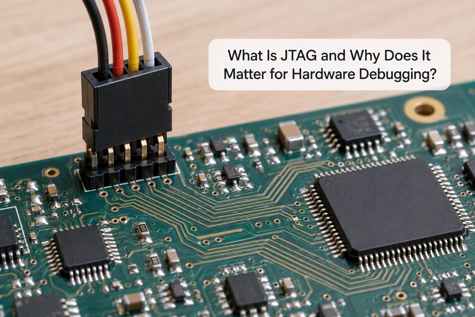
JTAG is a standardised serial interface for testing and debugging integrated circuits, specified in IEEE 1149.1. Each device with a Test Access Port exposes it, and a host tool uses that port to shift instructions and data in and out of registers the normal system bus cannot reach.
The name comes from the committee that wrote the standard rather than from the signals themselves. That is a common source of confusion: JTAG is the interface standard, and a probe such as a J-Link is one particular box that speaks it.
You will find it in four places. FPGAs and CPLDs use it to load a configuration bitstream into volatile memory. Microcontrollers use it to flash firmware and to halt, single-step and inspect registers. SoCs use it to reach cores that have no other working console. And assembled PCBs use it for boundary scan, which tests the solder joints without powering the functional circuitry.
It matters because it is non-intrusive. Nothing in your firmware has to run, no serial port has to work, and no RAM is consumed by monitor code. During bring-up that is the difference between debugging a board and staring at a dark LED.
JTAG Basics for Hardware Debugging: The Four Signal Lines
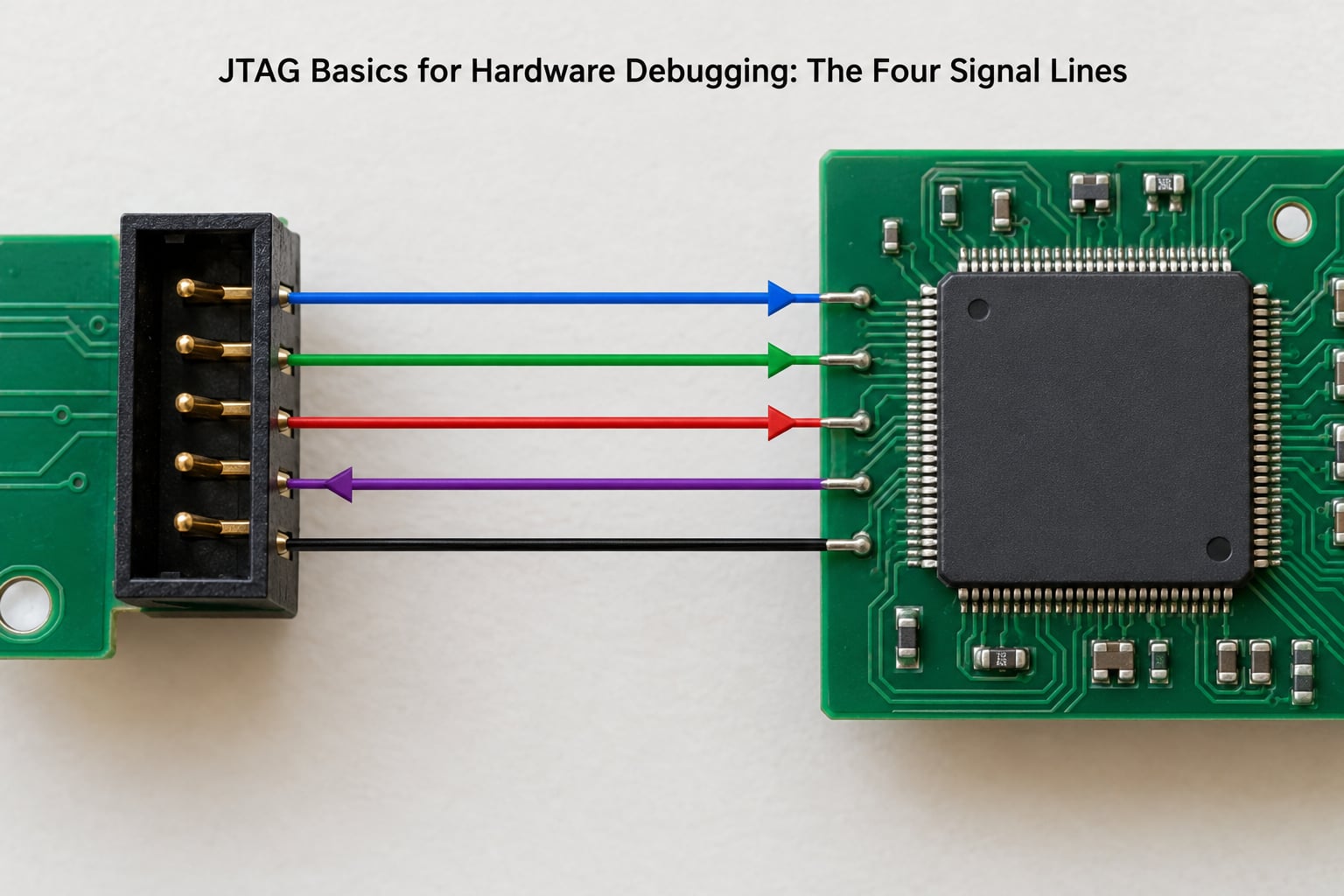
Most of the difficulty with JTAG wiring comes from counting pins wrongly. The standard interface uses four required signals, and a fifth optional one, plus a reference voltage pin on the probe side. In practice you often see six, seven or ten pins on a Cortex header because power and ground share the connector.
| Signal | Direction (from probe) | Purpose | First thing to check |
|---|---|---|---|
| TCK | Out | Test clock. Every state change and every shifted bit is timed by an edge of this signal. | Scope the idle level and confirm the probe is generating edges. |
| TMS | Out | Moves the TAP controller between its sixteen states. This is the line that decides what the interface is doing. | Look for a pull-up so the chain idles in a known state. |
| TDI | Out | Serial data travelling into the first device in the chain. | Confirm it is not swapped with TDO at the connector. |
| TDO | In | Serial data out of the last device in the chain. | Trace it to the far end of the daisy chain, not the near end. |
| TRST# (optional) | Out | Active-low asynchronous reset of the TAP. Most tools drive TMS through the reset sequence instead and leave it unconnected. | Usually fine unconnected; check it if the chain behaves inconsistently. |
| VTREF (probe side) | In | Tells the probe the logic voltage of the target so its outputs are not over-driven. | Must match the target IO voltage, and must not be left floating. |
A useful mental model is SPI with an extra line. TCK is the clock, TDI behaves like MOSI, TDO like MISO, and TMS decides which register the chain is currently connected to. The difference is that JTAG has no chip select, so it needs the state machine instead.
How the JTAG TAP Controller Works
Inside every JTAG-capable chip sits the Test Access Port: a small finite state machine plus an Instruction Register, a set of Data Registers, and a boundary of scan cells around the device pins. A debug or test tool never talks to these directly. It manipulates TCK and TMS and watches TDO.
The state machine has sixteen states. Five of them do the real work: Test-Logic-Reset, Run-Test/Idle, Select-DR-Scan, Capture-DR, Shift-DR, Update-DR, and their instruction-register counterparts. Each TCK edge moves the machine one step along a path determined by the level of TMS, so one bit per clock walks it to any state you want.
The sequence for reading anything looks the same every time. Move to Test-Logic-Reset, load an instruction code into the IR by shifting, move to the Data Register path, shift the data out through TDO, then update. Hardware breakpoints, memory reads, flash writes and IDCODE queries are all the same mechanism with different instructions selected.
Three instructions matter for a beginner:
- IDCODE returns a device identifier. It is the fastest way to confirm a chip is alive and in the chain.
- BYPASS is a one-bit register inserted around a device so the chain length stays manageable.
- SAMPLE/PRELOAD captures the current pin state into the boundary scan register without disturbing the running logic.
Several chips can be daisy-chained, and their TDO feeds the next chip’s TDI. Data shifted in at the probe passes through every device and comes back out. This is why chain order matters: the tool has to know which device sits nearest the connector.
What Is Boundary Scan and When Should You Use It?
Boundary scan is the manufacturing and board-test use of the same four wires. Each cell in a device’s Boundary Scan Register sits between the functional core and the physical pin, so a tool can drive a pin directly or sample what it is doing without starting the design.
In practice that means you can hold every output low, pull every input high, and see which ones respond. An open solder joint shows up as a pin that never changes, a short to a neighbouring net shows up as two pins that follow each other, and a wrong or missing part can be identified from its IDCODE.
This works on boards that will not boot, which is exactly why it belongs on the manufacturing line and on the bench during prototype bring-up. Functional test cannot help when the fault is why the board is dead. Boundary scan can isolate an assembly fault to a single net, and it does so with a fixture and a test program rather than with a rework technician and a scope.
JTAG debugging versus boundary scan
People conflate the two constantly, so it is worth being blunt about it. JTAG is the interface. Boundary scan is one job the interface can do, specified by a separate set of rules about how the cells around pins behave.
Same pins, different intent. A debugger halts cores and reads memory. A boundary-scan tester checks solder and connectivity. In production you often want both from one fixture: test the board first, then load the configuration or firmware through the same chain.
JTAG Basics for Common Hardware Debugging Tasks
Once the chain works, the session itself is repetitive. Most hardware debugging on a new board follows the same order, and each step tells you whether to keep going or go back to wiring.
Step 1 — Scan the chain. Ask the tool to identify every device it finds, in order. If you see the right part numbers in the right positions, the chain, the clock and the reference voltage are all working.
Step 2 — Run the TAP test. A good tool drives TMS through the reset sequence and reads IDCODE from each device. A failure here points at power, ground, the reference pin or the probe mode, not at your firmware.
Step 3 — Attach to the core. Here the JTAG interface hands over to the debug logic inside the chip, commonly a CoreSight Debug Access Port speaking ADIv5 on Arm parts. The stack below it is usually OpenOCD or a vendor GDB server, with GDB on top.
Step 4 — Set a breakpoint and inspect. Set a hardware breakpoint at a line or address that runs early, halt the core there, then read registers, memory and peripheral state. If you never hit it, move the breakpoint earlier in the reset path.
Step 5 — Program the device. When the session is stable, write flash or load a bitstream over the same chain. Programming over JTAG works on a board whose firmware is dead or missing entirely, which is the reason to keep the pins routed out to a header.
Most engineers live in steps 3 and 4. It helps to know that step 5 usually needs no additional hardware, because a probe that can halt a core can normally write the flash beside it.
How to Troubleshoot Common JTAG Problems
Nearly every forum thread about JTAG is really about one failure: the tool will not detect the target. The table below covers the causes I would check, ordered from cheapest to most expensive.
| Symptom | Likely cause | What to do |
|---|---|---|
| No devices detected at all | Missing ground, unpowered target, or VTREF floating | Confirm ground continuity, then check the target voltage against VTREF before anything else. |
| Detects devices but in the wrong order | Chain order in the tool config does not match the board | Compare the detected order with the schematic and correct the chain list. |
| Works at low clock, fails at high clock | Signal integrity, long flying leads, wrong probe voltage | Drop the scan clock to a few MHz and shorten the cable before blaming the tool. |
| Target not responding on an Arm board | Probe defaulting to SWD while the board is wired for JTAG, or the reverse | Switch the interface mode in the probe software and rescan. |
| Chain scan unstable or intermittent | No pull-up on TMS, or TDI and TDO crossed | Add a pull-up on TMS and check orientation at the connector with a continuity check. |
| Connected once, now never | Readout protection or security fuses burned on the MCU | Check whether option bytes or a fuse lock disabled the debug port; this looks identical to a wiring fault. |
| Only the nearest chip appears | Chain device not powered, or TDO of an earlier device not linked | Verify each device in the chain has its own reference and that TDO to TDI links are continuous. |
Two habits save most of this time. Scan at a low clock first, and always take a measurement before changing software. A multimeter on the reference pin and a continuity check on the connector take a minute and rule out half the possibilities.
What JTAG Tools and Adapter Features Do You Need?
The vocabulary around this is muddled, so let us separate the layers. A JTAG cable is a passive or nearly passive set of wires with a connector at each end. An adapter such as an FT2232 turns a USB port into two general-purpose serial channels you drive in software. A probe such as an XDS110, ST-Link, CMSIS-DAP or J-Link contains the real protocol logic and timing. Software sits on top: OpenOCD, a vendor GDB server, or a full IDE.
J-Link is not JTAG. It is a widely used probe that speaks JTAG, SWD and other protocols, so people say the words interchangeably when they mean different things.
JTAG versus SWD versus UART debugging
| Interface | Signals on target | Chaining | Typical speed | Best used for |
|---|---|---|---|---|
| JTAG | 4 required plus optional reset | Yes, daisy-chain many devices | Commonly a few MHz for debug | Multi-device boards, boundary scan, non-Arm parts, FPGA configuration |
| SWD | 2 signals plus reference | No | Often faster than JTAG on the same device | Arm Cortex-M and Cortex-R targets, where pins are scarce |
| UART printf | 2 signals plus ground | No | 115200 baud typical | Cheap runtime logging once a console exists |
For a single Arm microcontroller, SWD is usually the better choice: fewer pins, less board space, no chain to get right. JTAG earns its place when you have several devices to chain, when you need boundary scan on the board, or when the part is not an Arm core at all.
On the probe side, look for reference voltage detection, an adjustable clock rate, chain scanning with device identification, boundary-scan support, and drivers for the device families you actually use. Multi-core synchronised debug matters if you halt several cores together; trace support matters if you want execution history rather than a stop-the-world snapshot.
Beginners usually want the probe that ships with the vendor IDE for their first part, then a probe with wider multi-architecture support once they move to a board that mixes an MCU, an FPGA and a custom ASIC.
Frequently Asked Questions
What are the basic principles of JTAG debugging?
JTAG debugging rests on a small state machine inside the target called the Test Access Port. A probe moves that machine with TMS while TCK times every step, then shifts instructions into the Instruction Register and data through the Data Register. Because the state machine and registers are separate from the running system, the core can be halted, inspected and restarted without the firmware knowing anything happened.
What is JTAG debugging used for?
It is used to halt a processor, single-step through code, set breakpoints, read and write registers and memory, and program flash or FPGA configuration. Because it needs no working serial port, bootloader or operating system, engineers rely on it during prototype bring-up, crash investigation and manufacturing test, including on boards that never boot.
What is the difference between JTAG and SWD?
JTAG is a four-signal serial interface that supports daisy-chaining several devices in one chain and is the basis for boundary scan. SWD is a two-signal Arm alternative that talks to a single debug port, needs no chain, and is usually faster on the same chip. On Arm Cortex targets SWD saves board space; JTAG is needed when you chain devices or test interconnects.
Is J-Link the same as JTAG?
No. JTAG is the IEEE 1149.1 interface standard implemented inside the target chip. J-Link is a specific debug probe from SEGGER that speaks JTAG, SWD and other protocols to that interface. Buying a probe named after a protocol does not give you the interface itself, and the target chip must support the protocol you select.
Why will my JTAG probe not detect the target?
In order of likelihood: no common ground, a target that is not powered, a VTREF pin that does not match the target logic voltage, TDI and TDO swapped, a missing pull-up on TMS, or a probe defaulting to SWD while the board is wired for JTAG. Readout protection on the chip looks identical to a wiring fault, so check option bytes before rewiring.
Does a successful JTAG connection prove the board is correct?
No. It proves the probe can reach the chain, the reference voltage is right and the devices respond to IDCODE. It says nothing about whether the power rails, the memory, the clock or the peripherals work. Many board faults leave the debug port perfectly healthy, which is why boundary scan on interconnects and functional test still matter after a clean chain scan.
Conclusion: Start With a Simple JTAG Chain Check
If you have a new board in front of you, work outward from the cheap checks. Confirm the board is powered and that the probe shares a ground with it. Check the reference voltage matches the target IO level. Verify the four signals land on the pins the schematic says, in the right order. Then set the scan clock to something slow and ask the tool to identify the chain.
Compare the devices it reports with what the documentation says should be there. If they match, you have a working JTAG connection and can move on to attaching a debugger. That single step separates most wiring mistakes from actual software problems, which is why it is the first thing to learn.