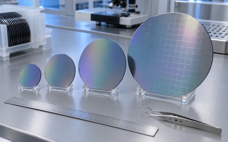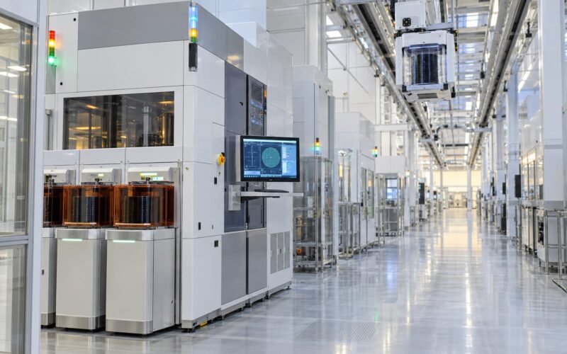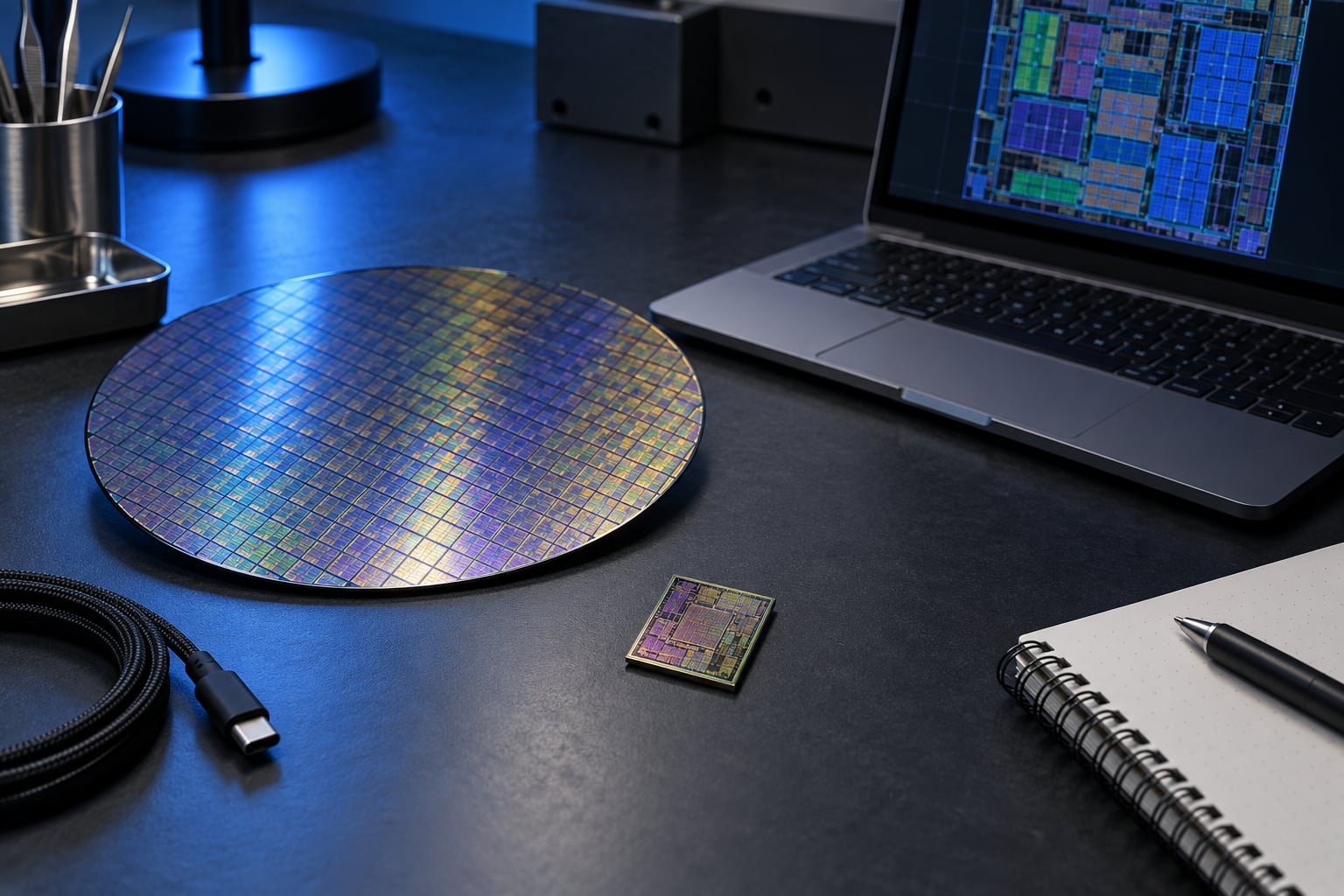
Students get chips fabricated by joining a shared wafer run, almost always through a university program or an open shuttle service, where dozens of designs share one mask set and split the cost. A course shuttle can cost nothing, an open shuttle a few hundred dollars, a research run low thousands. You supply a verified layout file; a foundry supplies the silicon.
The part that trips people up is not the manufacturing. It is the deadline structure around it. Shuttle calendars are published months ahead and they do not move for a thesis defense, so choosing a route early matters more than choosing the cleverest node.
Table of Contents
- What students can get a chip fabricated through
- What You Need Before You Start
- The vocabulary you will meet on day one
- Your prerequisites
- Decide whether you need a chip at all
- Step-by-Step: From Design to Working Silicon
- How to get a chip fabricated with a student-friendly process
- Prepare and verify the design
- Choose a foundry, PDK, and manufacturing package
- Create the fabrication package
- Submit the design and manage the tape-out
- Receive the wafers, probe, package, and test
- Common Mistakes That Cost Students Real Money
- Frequently Asked Questions
- Can a student get a chip fabricated with a laptop?
- What is the easiest fabrication process for students?
- How much does it usually cost for a student to fabricate a chip?
- How long does it take to get a student-designed chip manufactured?
- What is an MPW, and is it suitable for a first chip?
- What should students do if their first fabricated chip does not work?
- Conclusion: Three Things to Do First
What students can get a chip fabricated through
Five routes cover almost every student situation, and they differ far more in cost and access than in difficulty:
- Your university’s course shuttle. Many VLSI courses tape out a student design at the end of term, with the cost covered by the department or a teaching grant. Eligibility is usually enrolment in that specific course.
- A university MPW or shuttle relationship. Bigger programmes buy scheduled runs through intermediaries such as MOSIS or Europractice and pass the slot down to students. Some offer several nodes to choose between.
- An open shuttle service. Tiny Tapeout and similar services sell a small fixed tile on a shared run with an open-source toolchain and no NDA. This is the most accessible route for someone with no university programme at all.
- A university cleanroom or nanofabrication facility. Relevant mostly for MEMS, microfluidics, photonics and other non-CMOS work, where you fabricate the device yourself rather than submitting a layout.
- A direct commercial MPW or full-custom run. Real, available, and priced for companies. Rarely the right answer for a student.
What You Need Before You Start
Six things have to be in place before a submission can succeed, and three of them cost nothing to sort out.
The vocabulary you will meet on day one
Tapeout is the moment you commit a layout to manufacturing: the mask set is ordered and money is spent, after which changing your design means starting over. A multi-project wafer (MPW) or shuttle run is a scheduled fabrication run where many independent designs are placed on one wafer and the mask and wafer cost is divided between them. A process design kit (PDK) is the foundry’s rulebook for one process, containing the cell libraries, device models, layer definitions and design rules your tools need.
GDSII is the layered layout format the fab reads. DRC (design rule check) checks your layout against the process rules for spacing and density; LVS (layout versus schematic) checks that the layout matches the netlist you intended. A die is one copy of your circuit cut from the wafer, and the pad ring is the metal frame of bond pads around it that the packaging and test equipment contact.
Your prerequisites
You need a design that already simulates clean, a target process with a PDK you can actually install, tools that run on hardware you own, a budget that covers fabrication plus packaging plus testing, a packaging plan, and a test strategy written before submission rather than after.
On tooling, the open-source path is genuinely usable now. Verilator and Icarus Verilog handle simulation, GTKWave shows the waveforms, cocotb lets you drive your design from Python, and Yosys plus OpenROAD cover synthesis and place-and-route against the SkyWater SKY130 and IHP SG13G2 PDKs. OpenLane wraps much of that flow into one script, and Magic handles layout editing and some sign-off checks.
The distinction that matters for planning is simple. A simulation-only project needs a laptop, a simulator and a testbench, and finishes in weeks. A physical chip needs all of that plus a PDK, a shuttle slot, a package, a carrier board or test fixture, and months of calendar time you do not control.
Decide whether you need a chip at all
An FPGA reproduces your design on the day you finish the code, and a PCB gets you a working board with test points and rework capability. Neither has random power-on state, clock ceilings, or fixed pad rings. For anything with a tight deadline, a high-speed interface, or a lot of debugging ahead, the FPGA is often the right tool.
A tape-out pays off when the answer itself has to be silicon: a research measurement, an accelerator for a paper, a demonstration for a thesis defence, or a design you want to put in front of an employer. Being honest about which one you are keeps you from spending a term debugging a pad frame instead of learning anything.
Step-by-Step: From Design to Working Silicon
How students can get a chip fabricated comes down to six stages with a deliverable and a checkpoint at each one. Miss the checkpoint and you will find out later, from a foundry engineer, in terms you may not understand.
How to get a chip fabricated with a student-friendly process
Choose the process from four constraints in this order: what PDK you can install, what your course or programme already offers, how small a die you can fit in your budget, and how often the shuttle runs. Start with the constraint you cannot move.
| Route | What it costs a student | Typical process | Who qualifies | Turnaround | Best fit |
|---|---|---|---|---|---|
| University course shuttle | Often nothing, paid by the department | Course-defined, usually a mature node | Students enrolled in that course | Fixed by the instructor | Class projects and first-timers |
| University MPW via MOSIS or Europractice | Low hundreds to low thousands, sometimes subsidised | Mature nodes through advanced nodes depending on the programme | Enrolled students and staff at partner universities | Several months per slot | Thesis and capstone work |
| Open shuttle such as Tiny Tapeout | A few hundred dollars per tile | Open 130nm-class and similar processes | Anyone, no affiliation needed | Several months, published deadlines | Independent students and hobbyists |
| University cleanroom access | Training and consumables charges | MEMS, microfluidics, photonics | Enrolled students who complete safety training | Weeks to a few months | Non-CMOS device work |
| Commercial MPW or full custom | Thousands to six figures | Wide range including advanced nodes | Businesses with contracts | Months to over a year | Not usually students |
Two real examples of what the choice looks like. In one university PLL project, students could pick between an 180nm process from XFAB and a 22nm process from GlobalFoundries, because the university held slots in both. On an open shuttle, the process is fixed for you: SkyWater 130nm is what that service runs, with a tile of roughly 160 by 100 micrometres and additional tiles purchasable.
Plan the deadline backwards from whatever date actually matters. Shuttle schedules are published well in advance and shift, so treat any date you read as provisional and confirm it directly with the service. Work backwards from a defence date to that shipping date, then back through design, sign-off and packaging, and you get your real submission deadline.
Prepare and verify the design
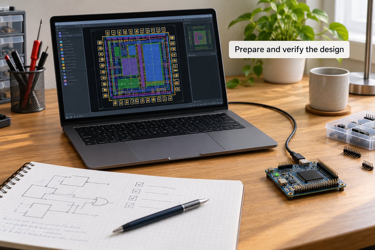
You start in RTL, either hand-written Verilog or SystemVerilog, or from a schematic if the design is analog or mixed-signal. Simulate it until the testbench passes, including the awkward cases: reset asserted, clock edge exactly at a register boundary, inputs at their extremes.
Then synthesise, place and route against your PDK, and run the two sign-off checks. DRC finds geometry the process cannot manufacture. LVS finds the expensive bug class where your layout is fine but does not match the netlist, so the chip has the wrong function and no error message tells you. Run extraction and post-layout timing analysis too, because the routed design is slower than the estimate you simulated against.
Power and pads come next, and both are where students get caught. Plan the pad ring against your package’s pin count before you place logic, not after. Include enough test structures that a failure can be localised: a scan chain if the process offers one, ring oscillator or delay chains for timing, and structures that isolate memory from logic.
Your checkpoint is a clean sign-off run with no outstanding violations and a timing report that meets your target with margin. Also verify the design in an FPGA or on a cheap development board first. A student who taped out a speech chip clone did exactly that and it cost a board rather than a shuttle slot.
Choose a foundry, PDK, and manufacturing package
The foundry builds the wafers. The PDK tells your tools how that foundry builds them. The MPW service places your design beside other students’ designs on a shared mask set and handles the commercial relationship, payment and export paperwork. Separating these three roles makes the choice much easier.
Compare routes on four things. Accessibility decides whether you can get in at all. Process maturity decides how forgiving the rules are: older nodes have denser rules but a physical, understandable device model and far better open tooling. Support decides who answers your email when a sign-off check fails at midnight. IP constraints decide whether you can use the cores or analog blocks you assumed were available, because PDKs for research processes often ship with restricted or absent libraries.
Research routes such as MOSIS and Europractice give a wider node choice and real support, and require an affiliation plus often an agreement. Open shuttle services give almost no support but also almost no paperwork, and they impose fixed I/O. Commercial foundries give you the whole toolset and charge for all of it.
Create the fabrication package
Your submission is usually a small bundle: the GDSII layout, the netlist or schematic in the expected form, a pin and pad definition file, timing and area constraints, the test structures, the package type you want, and the foundry’s own forms covering design ownership and licensing.
Some services want documentation instead of extra files. Describing your design in a structured way so a datasheet page generates itself from it is a small effort that produces the artifact people remember you for. A contributor card, a licence, and a short description of what the chip does turn a tape-out into a portfolio piece rather than a chip in a drawer.
The checkpoint here is submission-readiness. Never submit an unverified design. DRC and LVS clean, timing closed, power grid connected, and every test structure you claimed in the documentation actually present in the layout.
Submit the design and manage the tape-out
Create the account, accept the licence terms, and be ready for an NDA. University EDA tools frequently sit behind an NDA on a school server, which is why forum help for those flows is thin. Open-source flows sidestep the problem entirely.
Payment follows review, review follows submission, and submission sits behind a fixed deadline. Expect one or more rounds of manufacturability questions from an engineer: a density violation on a metal layer, a pad whose spacing is legal but awkward for the bonder, a clock that assumes a route the process cannot promise.
When a clarification comes back, treat it as the system working. Answer precisely, regenerate the affected layers, and re-run sign-off before resubmitting, because a partial fix often creates a new violation somewhere else. Keep your repository clean with a commit per sign-off stage so you can roll back to the last known-good state instead of debugging forward.
Receive the wafers, probe, package, and test
On the foundry side, the remaining steps are fixed: mask generation, wafer fabrication, back-end of line, wafer probe, dicing, packaging, and final test. Your designs come back packaged, often in an array in a carrier, sometimes with a development board if the service supplies one.
Plan the bring-up before the chips arrive. Design the fixture: a breakout board, a supply with enough headroom, a scope, and a way to drive every clock and reset line. Know what a dead chip looks like on the bench so you can tell a wiring mistake from a silicon one in the first ten minutes.
Failures cluster in predictable places. A design with no explicit reset comes out of the fab with random power-on state and may never start, because ASIC flip-flops power up with undefined values and initial-value statements are not permitted in silicon. One student documented a design that passed every functional check and then failed the gate-level test with undefined outputs for exactly this reason; the fix was an explicit active-low reset.
Fixed pad rings cause the second cluster of problems. When the shuttle supplies the I/O, you are limited to its pin count, its voltage levels and its fixed tile. On an open shuttle the logic pins run at 3.3V and are not tolerant of 5V inputs, and the clock supplied by the on-board microcontroller has a ceiling around 50MHz. Design to those numbers from the first line of RTL, not after a week of silent failures.
Common Mistakes That Cost Students Real Money
Each of these has taken a shuttle slot from someone. None of them are hard to avoid once you know they exist.
- Picking a process with no usable PDK. If you cannot install the design rules and cell libraries, you cannot sign off, so the run is wasted before it starts. Fix: confirm the PDK and tool chain exist and run on your machine before writing any RTL.
- Skipping DRC or LVS to save a week. DRC violations mean the fab cannot build your geometry. LVS mismatches mean you built the wrong circuit cleanly. Fix: treat both as blocking, and keep the reports in version control.
- Assuming power-on state will be zero. It will not, and there is no initial-value statement in silicon. Fix: design an explicit reset and prove it works in gate-level simulation, not just in RTL.
- Budgeting only for fabrication. Mask set, wafer, packaging, carrier board and test time are separate line items, and the extras often exceed the wafer share for a small student design. Fix: get the full quote before you commit, and reserve budget for a second run.
- Leaving out test structures. Without them, a non-working die tells you nothing about why. Fix: add timing structures and a scan path if available, and document them.
- Forgetting the package in the design stage. Pin count and pad arrangement constrain the pad ring, and the ring constrains the floorplan. Fix: choose the package first and check pad capacity against your die size.
- Missing the submission deadline. Shuttle dates are immovable, and a missed slot costs a full term or an entire thesis cycle. Fix: put the deadline in your calendar the day you pick the run and work backwards from there.
- Designing too large for the budget. Die area drives cost, and a tile you cannot afford is a project you cannot submit. Fix: cut the design until it fits comfortably, then spend the savings on a second run.
- Discovering the fixed pad ring late. Custom I/O, unusual pin counts and analog inputs are simply not available on most open shuttles. Fix: read the pad specification before designing, or use a route with your own I/O if yours is genuinely unusual.
Two habits prevent most of the list. Run the full flow once on a small block before your real design, and keep a written bring-up plan next to the testbench. Students who taped out successfully generally describe the same habit: they used the open-source checks continuously instead of saving them for the end.
Frequently Asked Questions
Can a student get a chip fabricated with a laptop?
Yes, for open processes. The SkyWater SKY130 and IHP SG13G2 PDKs, along with Yosys, OpenROAD, Verilator and Magic, all run on a reasonably modern laptop. You need a few gigabytes of memory for place-and-route and a working install of the PDK. What a laptop cannot do is replace a foundry. Simulation, synthesis, layout and sign-off are all fine at your desk; manufacturing happens somewhere else entirely.
What is the easiest fabrication process for students?
A 130nm-class open process on a shuttle service is the easiest, mainly because the PDK, the design rules and the tools are free and documented. Older nodes have stricter spacing rules but they are well documented, and their device models behave the way a textbook says they should. For analog or mixed-signal work, university cleanroom access is often easier than fighting a digital tile’s fixed pad ring.
How much does it usually cost for a student to fabricate a chip?
Four tiers matter. A university course shuttle often costs a student nothing. An open shuttle service runs a few hundred dollars per tile. A research MPW through MOSIS or Europractice lands in the low thousands, with European university-linked foundries quoting roughly a thousand to fifteen hundred euros for about a hundred chips to students. A proprietary commercial MPW runs into the six-to-seven-figure range and is not a student option.
How long does it take to get a student-designed chip manufactured?
Count in months, not weeks. Documented first tape-outs have closed submissions in one autumn and had the chip and carrier arrive roughly nine months later. Shuttle services publish deadlines months ahead and the foundry process itself takes weeks, so your real job is scheduling: pick a run whose shipping date still leaves room for testing before your deadline.
What is an MPW, and is it suitable for a first chip?
A multi-project wafer run is a scheduled fabrication run that places many independent designs on one wafer and splits the mask and wafer cost between them. It is well suited to a first chip because the economics assume small dies and nobody expects production quality. The trade-off is that you get whatever area fits your budget and a fixed pad ring, so plan the floorplan around the space you can afford.
What should students do if their first fabricated chip does not work?
Work the test structures before touching the logic. They will tell you whether the process is slow, the pads are unconnected, or the core simply has a bug, and that distinction saves weeks. Read a datasheet for another project on the same process to check your voltage and clock assumptions. Then fix the design and book the next shuttle slot, keeping enough budget for the second run from the start.
Conclusion: Three Things to Do First
Choose your process and PDK before you write any RTL, because that decision sets your tools, your pad ring, your die area and your deadline. Then validate hard: clean DRC, clean LVS, closed timing, an explicit reset, and a gate-level simulation that passes rather than one you hope passes. Third, budget for fabrication, packaging, testing and a possible respin, and use your university’s programme or a small open shuttle for the first one.
Students who have done this describe the same arc: a small digital block first, then a RISC-V core or a sensor driver, then a design you can point at and say they built. The bar for getting a chip fabricated is lower than most people assume, and the timeline is the only part that stays out of your hands. Pick the run early and the silicon follows.
Last updated for 2026. Shuttle schedules, available nodes and service pricing change regularly, so verify dates and costs directly with the program before you commit.