Leakage current in modern chips explained in one line: it is the current a CMOS chip draws from its supply even when every transistor in it is logically off. It comes from weak-inversion channel conduction, quantum tunnelling through the gate dielectric, and reverse-biased junction current, and multiplied by the supply voltage it becomes static power that burns whether or not the chip is doing useful work.
That last part is why engineers talk about it so much. Switching power disappears when a circuit stops switching; leakage power does not. In this guide I walk through where each leakage path forms inside a transistor, how the paths behave as nodes shrink, how they are measured on real silicon, and which design techniques trade speed for milliwatts.
Table of Contents
- What Is Leakage Current in Modern Chips?
- Why Do Transistors Leak When They Are Off?
- The Main Sources of Leakage Current
- Subthreshold conduction
- Gate oxide tunnelling
- Junction and band-to-band tunnelling
- Drain-induced barrier lowering and gate-induced drain leakage
- Interconnect and defect leakage
- How Leakage Changes as Chips Become Smaller
- Leakage Current in Modern Chips: Subthreshold, Gate, and Junction Leakage
- How Engineers Measure Leakage Current
- Why Leakage Current Affects Power, Heat, and Battery Life
- How Chip Designers Reduce Leakage Current
- Process and device level
- Circuit level
- Architecture and system level
- Leakage, Dynamic Power, and Total Power in a Simple Example
- Key Takeaways for Chip Design and Semiconductor Study
- Frequently Asked Questions
- What causes electrical leakage current?
- What is reverse leakage current in a diode?
- What is leakage power dissipation?
- What is a leakage current tester?
- Does leakage current affect chip performance?
- Why does leakage current increase as transistors get smaller?
- Conclusion: Start With Measurement, Then Control the Source
What Is Leakage Current in Modern Chips?
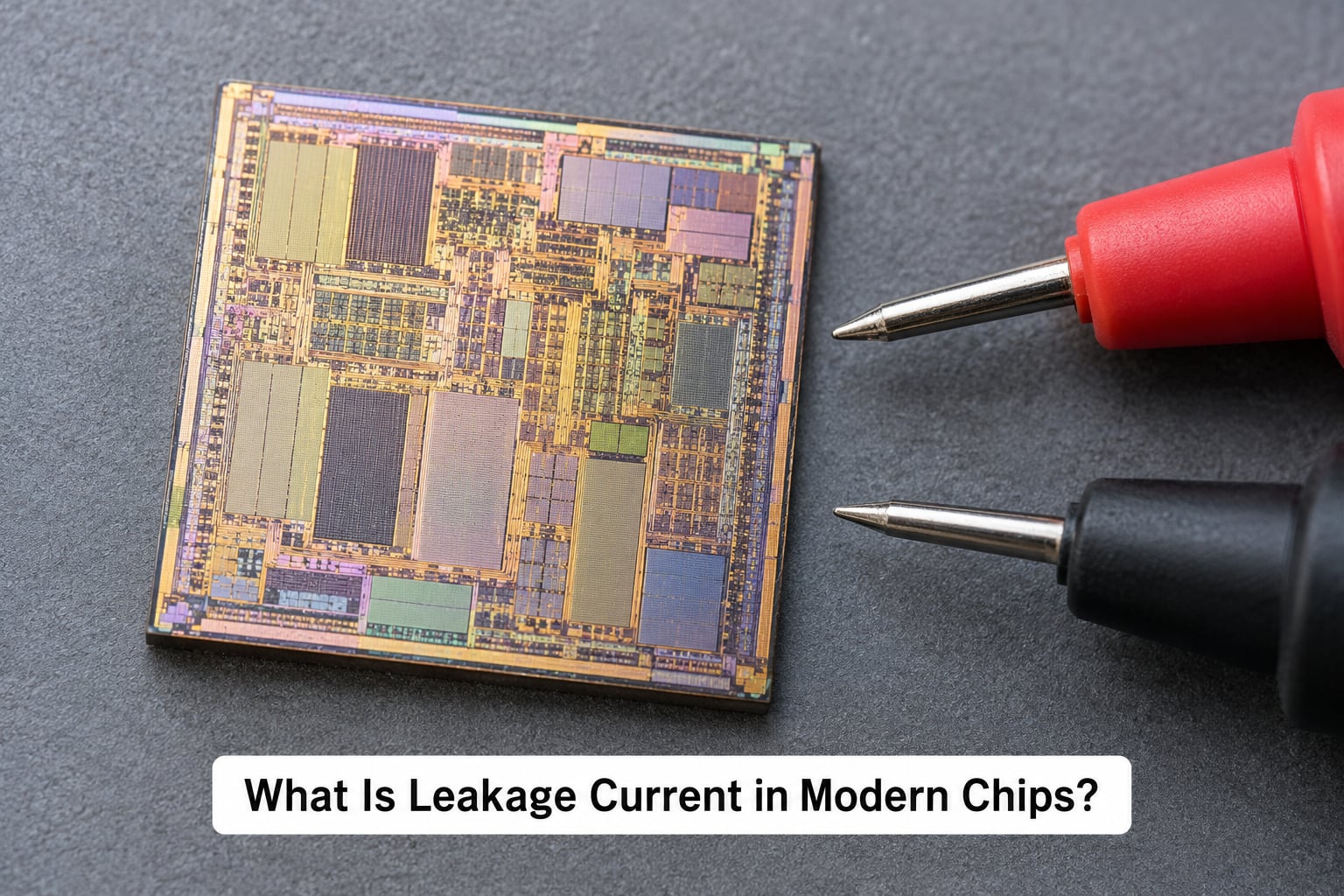
Leakage current in modern chips is the residual current that flows through a transistor or circuit when it is meant to be off. Multiply it by the supply voltage and you get leakage power, a floor under chip power that exists at every clock frequency, including zero.
The distinction that matters is between two currents. Switching, or dynamic, current is the useful current a transistor carries while it changes state, charging and discharging the capacitances attached to its terminals. Leakage current is everything else: the small currents that have no useful function but still dissipate energy.
Leakage shows up in the situations where you would expect a quiet chip to be perfectly still. A gate held below its threshold voltage still passes current, a reverse-biased junction still carries minority carriers, an insulating oxide layer still leaks under the right conditions, and a biased input pin still couples into adjacent circuitry.
In a battery-powered device that floor is what people notice. A phone sitting in a pocket all night is not switching anything, yet it drains measurable charge. An IoT sensor that wakes once a minute can spend most of its time doing nothing and still owe a bill for that doing-nothing.
Why Do Transistors Leak When They Are Off?
An off transistor is not a switch that has clicked to a clean stop. Its gate voltage sits below the threshold voltage, but the channel underneath is never completely free of charge carriers, and a small population of them stays in the surface and moves from source to drain.
That weak-inversion population behaves in a distinctive way. Increase the gate voltage while it stays below threshold and the current rises by roughly a factor of ten for every 60 millivolts, a behaviour device engineers describe as a subthreshold slope of about 60 mV per decade. Ten millivolts of gate overdrive is a rounding error in a logic circuit and a factor of two in leakage.
The second reason has to do with the barrier itself. An insulating layer blocks current because electrons do not have enough energy to cross it classically. When the barrier is thin enough, some electrons tunnel straight through it, a purely quantum effect that becomes more likely as the dielectric thins.
Junctions contribute a third path. The source and drain form p-n junctions into the substrate, and in normal operation those junctions are reverse biased. A reverse-biased junction is not a perfect block; it carries a small reverse current driven by minority carriers thermally generated in the depletion region.
All three paths are temperature dependent, and reversely so. Heat generates more minority carriers, which is why leakage roughly doubles for every 10 degrees Celsius near typical junction temperatures, a rule of thumb whose exact factor depends on threshold voltage and transistor design.
The Main Sources of Leakage Current
Device-level leakage in a modern CMOS chip falls into a handful of recognizable mechanisms, and engineers name them because each one responds to a different set of fixes.
Subthreshold conduction
This is the weak-inversion channel current described above, and at advanced nodes it is usually the largest single contributor. It is controlled almost entirely by threshold voltage, which makes it the leakage mechanism that design and library work attack first.
Gate oxide tunnelling
Electrons tunnelling through the gate dielectric, either directly from one electrode to the other or through trap-assisted paths inside the oxide. This term grew as dielectrics were thinned for capacitance and only fell back sharply once high-k dielectrics with metal gates entered production in the late 2000s, because a physically thicker high-k layer with the same capacitance blocks tunnelling better than a thin silicon dioxide one.
Junction and band-to-band tunnelling
The reverse current across source-drain and source-body junctions, including the minority-carrier diffusion current that dominates at moderate reverse bias and the band-to-band tunnelling current that grows sharply at higher reverse bias. It is temperature sensitive and it worsens as junctions get more heavily doped and shallower, both of which happen when node dimensions shrink.
Drain-induced barrier lowering and gate-induced drain leakage
Drain-induced barrier lowering (DIBL) describes the drain electric field pushing the source-side barrier down, which lets carriers leak into the drain even when the gate is off. Gate-induced drain leakage (GIDL) is the related field-driven current from drain to source when the channel is off, generated by band-to-band tunnelling at the drain end. Both are short-channel effects, and both scale with how close the drain sits to the gate.
Interconnect and defect leakage
At the chip level there are also paths that are not a single transistor: gated structures such as SRAM cells and analog bias circuits, pass-gate and ESD clamp paths that conduct on signal transients, and finally defect leakage such as stress-induced leakage current through a damaged gate oxide. That last category is a manufacturing problem rather than a physics one, and it is what leakage-sensitive production test is designed to catch.
How Leakage Changes as Chips Become Smaller
Scaling does not simply raise leakage, but it has raised it, and the reason is worth stating precisely rather than waving at.
Leakage is exponentially sensitive to threshold voltage, so any decision to lower Vt for speed is also a decision to multiply leakage. Supply voltage scaling used to give designers room: as voltages fell, threshold voltages could fall with them while holding a constant off-state current. That headroom largely closed up during the 2000s.
The result is the threshold-voltage scaling wall. Holding Vt flat for reliability while supply voltage kept falling would demand transistors so slow that clock frequencies stalled, so designers instead let Vt fall too and paid for it with rising static power and multi-Vt libraries.
Channel length shrinking attacks leakage from another direction. Shorter channels give the drain field more influence over the barrier, which is DIBL, and GIDL rises with the same trend. At the same time the gate dielectric thinned to keep capacitance up, which raised tunnelling until high-k dielectrics arrived to blunt it.
Device geometry pushed back as well. FinFETs gave the gate control over three sides of a narrow fin, and gate-all-around (GAA) nanosheets wrapped it on all four, which improved electrostatic control, raised the achievable threshold voltage, and lowered leakage compared with the planar devices they replaced. The counter-trend has been transistor count: more devices on a die means more leakage paths, so total chip leakage does not fall the way per-transistor leakage does.
Leakage Current in Modern Chips: Subthreshold, Gate, and Junction Leakage
The table below is the compact version most engineers keep in their heads. For each mechanism: where the current physically flows, what governs its size, and the circuit condition that makes it the thing to worry about.
| Mechanism | Where it flows | What controls it | Watch it when |
|---|---|---|---|
| Subthreshold conduction | Source to drain through weak-inversion channel | Threshold voltage, temperature, subthreshold slope | Low-Vt or high-performance cells run hot or idle |
| Gate oxide tunnelling | Through the gate dielectric | Dielectric thickness and material, electric field | Thin-oxide devices or any path with large gate bias |
| Junction and band-to-band tunnelling | Reverse-biased source/drain and body junctions | Doping, junction depth, reverse bias, temperature | Raised temperature, analog biasing, deep off-state |
| DIBL and GIDL | Source to drain and drain to source under field | Channel length, drain bias, gate-drain spacing | Short channels and aggressive drain voltages |
| Interconnect and defect paths | Through cell structures, clamps, damaged oxides | Signal levels, ESD networks, process defects | Production test and yield analysis |
Two distinctions from chip-level leakage keep surprising people. First, chip leakage is not stray current or a fault current; it is normal and present in a perfectly healthy device. Second, off-state current (Ioff) and quiescent current (Iddq) are related but not identical measurements, and the difference matters once you start looking at production test data.
How Engineers Measure Leakage Current
Leakage measurement falls into two families: static characterisation, which captures the current a block draws when it is not switching, and dynamic characterisation, which watches how that current moves with activity and supply voltage.
Static measurement usually means holding a pattern or state on the design’s scan chain, applying a known supply voltage, and reading the current the supply delivers. Because the number depends on the data pattern, engineers sweep vectors, voltages and temperatures rather than reporting one figure.
Temperature is the part most often skipped in a summary datasheet and the part that matters most. A chip characterised at room temperature can show several times that current at its maximum junction temperature, so any leakage number without a temperature corner is incomplete.
Production screening uses Iddq testing, which measures quiescent supply current with the core held in a static state and flags anything above a limit as a likely defect. Vectorless leakage monitors and MBIST-style structures do similar work on-chip, sometimes converting leakage to a time interval so the measurement fits existing digital test infrastructure.
Common measurement errors are worth naming: unfilled unused pins that let current escape through protection diodes, floating inputs, marginal or noisy voltage sources, insufficient settling time after a pattern change, and instrumentation whose own leakage floor is above the current being measured.
This is also where chip-level measurement gets confused with the power-system kind. A leakage current tester, the instrument that shares the name, clamps around insulation or a grounding conductor to measure the residual current flowing where it should not be in an appliance or installation. Different quantity, different units of concern, different instrument.
Why Leakage Current Affects Power, Heat, and Battery Life
The translation is arithmetic. Leakage power equals supply voltage multiplied by leakage current, and because neither term moves during sleep, the result is a constant drain that no amount of clock gating removes.
That constant has three consequences. Die temperature rises, which raises leakage further, which raises temperature again; the effect is mild but real, and it is one reason idle chips are not exactly cold. Thermal design capacity gets spent on power that produced nothing, and in a data centre that capacity is what limits how many accelerators fit in a rack.
Battery life is where it is least forgiving. A device that sleeps for 99.9 percent of its life can still be dominated by static power during that sleep, and the same applies to always-on domains that retain a small block running for sensor, clock and wake logic.
Variability adds a second-order problem. Leakage varies from die to die because of microscopic dopant fluctuations and line-edge roughness, and because of the exponential relationship with Vt, a spread that looks small in volts becomes a large spread in watts. Teams that size thermal and battery budgets for the average die end up with outliers.
Past a certain point the constraint stops being engineering taste and becomes economics. Voltage could no longer be scaled down fast enough to hold total power flat while keeping switching power low, and the industry’s answer for a decade was to raise frequency and power until the power delivery and cooling networks became the limit. Leakage is a direct contributor to that ceiling.
How Chip Designers Reduce Leakage Current
Every mitigation costs something, usually speed, area or design effort. The useful question is which cost a given block can afford.
Process and device level
Higher threshold voltage from better channel engineering, high-k dielectrics with metal gates that permit a physically thicker barrier, halo doping to suppress DIBL, and FinFET or GAA geometry that gives the gate more control over the channel. Longer channel lengths work too, at the price of drive current.
Circuit level
Multi-Vt standard cell libraries let a design assign high-Vt cells to non-critical paths and low-Vt cells only where timing demands them. Power gating switches a whole block’s supply off with sleep transistors so its leakage falls to near zero, retaining state either in a separate always-on rail or in retention registers.
Architecture and system level
Body bias shifts threshold voltage at run time, letting a chip trade speed for standby leakage. Stack effect is the simplest trick in the book: series-stacking two off transistors halves the voltage across each and cuts their leakage sharply. Clock gating stops switching but not leakage, which is why it and power gating are complements rather than substitutes. Voltage and frequency scaling adjust total power continuously, and state assignment across power domains decides how much of the chip has to stay awake at all.
One persistent myth is worth retiring: higher Vt does not automatically mean lower total power. A high-Vt cell that is too slow for its path forces the clock down or the supply up, and the dynamic saving can exceed the leakage saving. Multi-Vt works because it assigns thresholds path by path, with timing closure proving each choice.
Leakage, Dynamic Power, and Total Power in a Simple Example
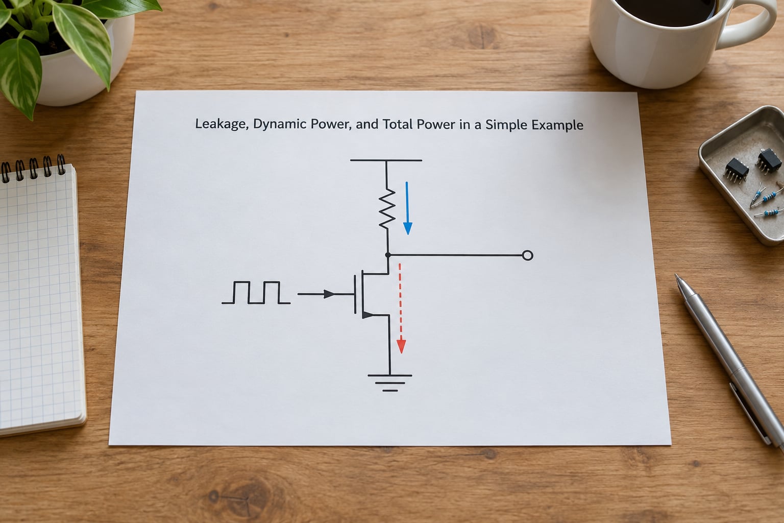
Here is a worked estimate using stated assumptions rather than any particular process. Assume a logic block at a 0.8 V supply, switching capacitance of 20 nF, total leakage current of 50 mA, and a switching probability of 5 percent per clock cycle.
Static power is straightforward: 0.8 V times 0.05 A is 40 milliwatts, constant at every frequency. Dynamic power follows the usual expression, activity times capacitance times voltage squared times frequency, which at those numbers works out to 0.64 nanowatts per hertz, or 0.64 milliwatts per megahertz.
| Clock | Dynamic power | Static power | Total power |
|---|---|---|---|
| 10 MHz | 6.4 mW | 40 mW | 46.4 mW |
| 62 MHz | 40 mW | 40 mW | 80 mW |
| 500 MHz | 320 mW | 40 mW | 360 mW |
| 1 GHz | 640 mW | 40 mW | 680 mW |
The crossover sits near 62 MHz, where the two terms are equal. Below it, this block is a leakage machine; above it, a switching machine. Doubling the supply voltage would multiply static power by two and dynamic power by four, which is the arithmetic behind voltage scaling giving way to frequency scaling.
Raise the temperature and the static column grows exponentially while the dynamic column barely moves. That asymmetry is why leakage dominates the corner cases a design has to survive, not the nominal one it is simulated at.
Key Takeaways for Chip Design and Semiconductor Study
Put the pieces in the order an engineer would actually work in them.
- Find the path. Identify which mechanism dominates in your design: subthreshold at high temperature, gate tunnelling on thin oxides, junction current in analog biasing, or defect paths in test data.
- Measure it properly. Characterise across supply voltage, pattern and temperature, and separate total supply current from leakage-only current.
- Cost it. Multiply by supply voltage, add it to the thermal budget, and check the maximum corner rather than the typical one.
- Mitigate in order. Assign thresholds, then gate power domains, then consider body bias, stack effect or longer-channel devices, verifying timing after each change.
For study purposes, the mechanism taxonomy is the part worth memorising. Almost every practical leakage question reduces to which of those five paths is carrying the current, because that determines which knob moves it.
Frequently Asked Questions
What causes electrical leakage current?
In a CMOS chip, leakage current comes from three main physical effects: weak-inversion conduction through the channel of a transistor whose gate sits below threshold, quantum tunnelling of electrons through the gate dielectric, and reverse current across biased source and drain junctions. Short-channel effects such as drain-induced barrier lowering and gate-induced drain leakage add to the total. In appliances and installations the cause is different: current taking unintended paths through insulation and parasitic capacitance, which is a safety concern rather than a static-power one.
What is reverse leakage current in a diode?
Reverse leakage current is the small current that flows through a p-n diode when it is biased in reverse, with the cathode more positive than the anode. It consists mainly of minority carriers thermally generated in the depletion region and swept across the junction by the electric field. At low reverse bias diffusion current dominates, while at higher reverse bias band-to-band tunnelling takes over and the current rises steeply. Because generation is thermally driven, reverse leakage roughly doubles for each 10 degrees Celsius of temperature rise.
What is leakage power dissipation?
Leakage power dissipation is the electrical power a circuit converts to heat purely from current it was not supposed to carry. It equals the supply voltage multiplied by the leakage current, and unlike dynamic switching power it does not fall when activity stops. For example, a block drawing 50 mA of leakage at 0.8 V dissipates 40 milliwatts continuously. In total power budgets it appears as a static floor that scales with device count, temperature and supply voltage, and that floor is what limits battery life in always-on and sleep-mode designs.
What is a leakage current tester?
A leakage current tester is a power-system instrument that measures residual current taking an unintended path, typically by clamping around a protective earth conductor or a supply line in an appliance or installation. It is used for electrical safety and insulation diagnostics, and readings are judged against standards that limit current by body-impedance category. This is not the same measurement as chip leakage characterisation, which reads supply current on silicon using Iddq tests, scan patterns or vectorless leakage monitors to report milliwatts of static power rather than milliamps of residual current.
Does leakage current affect chip performance?
Indirectly, and more than most people expect. Leakage does not slow a signal down, but it burns power, and power becomes heat. Once a chip cannot be cooled within its thermal design capacity, either the clock frequency drops or the die gets bigger, and both cost performance. Leakage also consumes part of the data-centre power budget, which limits how many accelerators fit in a rack. In portable designs the practical effect shows up as shorter battery life, especially in sleep and always-on modes where leakage is the only power being spent.
Why does leakage current increase as transistors get smaller?
Two reasons dominate. First, threshold voltage could not keep falling as supply voltages scaled down, so the off-state current that goes with a given Vt rose exponentially. Second, shorter channels let the drain electric field lower the source-side barrier, which is drain-induced barrier lowering, and raise gate-induced drain leakage. Dielectric thinning added a third term through tunnelling, until high-k dielectrics and FinFET or gate-all-around geometry reversed part of that trend. Per-transistor leakage is not rising uniformly; total die leakage still grows with transistor count.
Conclusion: Start With Measurement, Then Control the Source
If you take one thing away from this guide on leakage current in modern chips explained, make it the order of operations: understand the mechanism, measure the current under the voltage and temperature conditions that matter, cost it in watts and heat, then pick a mitigation that meets the design’s speed and area targets.
Start with measurement because the dominant mechanism is not obvious from the schematic. A block that leaks badly at temperature is usually subthreshold conduction and wants multi-Vt or power gating; a block that leaks at cold with a large gate bias may be tunnelling and wants a different fix. Guessing wrong wastes a tape-out.
And keep the framing honest. Leakage is normal, it is not a fault, and it is not going away. Managing it is a permanent line item in the power budget of every chip that ships, from a coin-cell sensor to an AI accelerator, and the designs that handle it deliberately are the ones that hit their battery and thermal targets.