Transistor aging is the gradual, time-dependent change in a transistor’s electrical behaviour under sustained electrical and thermal stress, driven mainly by charge trapped in or near the gate dielectric. This shifts the threshold voltage, reduces drive current and slows the circuit. Aging and wearout in transistors explained properly means separating slow drift from sudden failure — and that is where this guide starts.
The short version for a reader in a hurry: aging and wearout are not the same thing. Aging is measurable parameter drift you can often partially reverse by removing the stress. Wearout is accumulated physical damage that ends in a hard failure, usually a broken dielectric or an opened interconnect.
The rest of this article builds up from a thirty-second transistor refresher, through the five mechanisms that actually degrade devices, to the qualification flow that turns hours of stress testing into a ten-year field claim. If you are new to the topic, the first two sections are enough. If you sign off on silicon, skip to the detection and mitigation sections.
Table of Contents
- What Do Aging and Wearout Mean in Transistors?
- How Do Aging and Wearout Differ?
- What Physical Mechanisms Cause Transistor Degradation?
- Aging and Wearout in Transistors: Main Mechanisms
- How Does Electromigration Damage Transistors?
- How Do Hot Carriers Cause Transistor Aging?
- Why Does Gate-Oxide Breakdown Wear a Transistor Out?
- Which Transistor Types Are Most Vulnerable?
- What Accelerates Aging and Wearout?
- How Do Engineers Detect and Predict Transistor Wearout?
- How Can Designers Slow Down Transistor Aging?
- Can Aging and Wearout Be Reversed?
- Frequently Asked Questions
- Is transistor aging the same as transistor failure?
- What is the main difference between aging and wearout in CMOS transistors?
- Does turning a transistor off stop all aging mechanisms?
- How is transistor lifetime estimated from accelerated stress tests?
- Can modern nanoscale transistors last for the life of a product?
- Conclusion
What Do Aging and Wearout Mean in Transistors?
Wearout is real and it is measurable. A modern system-on-chip holds billions of transistors, many clock domains and several voltage domains, all running hot and fast for years. Something has to give eventually, and reliability engineers have spent five decades characterising exactly what.
Before the mechanisms make sense, one piece of vocabulary. A MOSFET is a voltage-controlled switch. The gate is a metal or conductive high-k electrode separated from the silicon channel by a very thin dielectric. Apply enough gate voltage and a conductive channel forms under the gate, connecting source and drain. The voltage at which that happens is the threshold voltage, Vt.
Three numbers describe how healthy the device is. Vt is the switch-on point. Drive current, Ids, is how much current flows once it is on. Leakage is the current that flows while it is nominally off. Aging moves all three: Vt drifts, drive falls, leakage rises. When the drift is large enough, the circuit misses its timing budget or burns too much idle power.
The equivalent oxide thickness, or EOT, is how thin the gate dielectric is expressed as a silicon dioxide equivalent. It matters here because a thinner dielectric means a stronger electric field for the same applied voltage, and stronger fields break bonds faster.
Reliability engineers plot the failure rate against time and get the bathtub curve. The curve has three regions, and working out which one the searches behind aging and wearout in transistors explained are really asking about saves a lot of confusion.
- Infant mortality. Early failures, falling off a cliff in the first hours or days. These come from contamination, processing defects and weak spots. Burn-in exists to weed these parts out before shipment.
- Random failures. A low, flat middle region where the hazard rate is constant. These are driven by extrinsic events such as ESD damage, latch-up or cosmic rays, not by gradual wear.
- Wearout. The rising right-hand wall, where the failure rate climbs as accumulated damage crosses a threshold. Transistor aging and dielectric breakdown live here.
A chip is designed so that the wearout wall arrives after the product has finished its mission. Ten years of automotive duty, fifteen in aerospace, five in a phone. Everything below is about how that arrival time gets calculated.
How Do Aging and Wearout Differ?
Age-related failure in CMOS falls into four buckets, and mixing them up leads to bad design decisions. The useful distinction is cause, reversibility and how the failure actually shows up in a circuit.
| Type | Primary cause | Reversible? | Observable effect | Circuit consequence |
|---|---|---|---|---|
| Aging (degradation) | Charge trapping at or in the gate dielectric under bias and heat | Partly, when stress is removed | Threshold voltage shift, lower drive current, higher leakage | Gradual slowdown, rising idle power, shrinking timing margin |
| Wearout (permanent damage) | Dielectric breakdown, electromigration voids, hard interface damage | No | Rising leakage to failure, resistance drift, then an open or short | Functional failure, often sudden and without warning |
| Transient degradation | Short stress pulses, radiation events, hot-plug transients | Usually, once the event passes | Temporary shift or single-bit error | Transient malfunction, in an SEU the system often recovers from |
| Catastrophic failure | ESD, latch-up, overvoltage, mechanical damage | No | Immediate loss of function or isolation breakdown | Sudden failure, screened out by production test |
Process variation sits outside this table on purpose. Variation is a spread in device parameters across a wafer or a die, fixed at manufacture and largely random. Aging is a shift in a specific device over time. A design can fail on either, and the same guard band usually has to cover both, but they are different problems with different fixes.
What Physical Mechanisms Cause Transistor Degradation?
Aging and Wearout in Transistors: Main Mechanisms
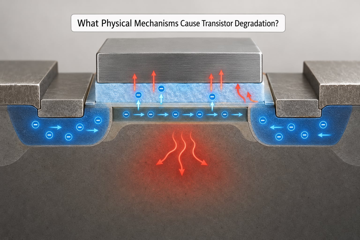
Five mechanisms account for almost all age-related failure in modern CMOS. Three damage the transistor itself, one chips away at the gate edge, and one tears apart the wiring around it.
- Negative bias temperature instability (NBTI). A PMOS gate held at negative voltage with the silicon at elevated temperature. Holes tunnel into the dielectric and become trapped, pushing Vt upward. Damage is partly recoverable.
- Positive bias temperature instability (PBTI). The same physics on an NMOS device under positive gate bias, with electrons trapped instead of holes.
- Hot carrier injection (HCI). Channel carriers accelerated by a strong lateral field gain enough energy to enter the gate oxide or the spacer edge, creating permanent interface traps.
- Time-dependent dielectric breakdown (TDDB). Progressive formation of a conductive path through the gate dielectric. The wearout event: the gate oxide finally shorts gate to channel.
- Electromigration (EM). Metal atoms migrating along the interconnect under electron wind force, leaving voids that grow into an open circuit.
Each one attaches to a specific parameter, and knowing the attachment point is what makes the mechanism useful in design rather than academic.
| Mechanism | Physical cause | Stress trigger | Affected device | Electrical signature | Recovery |
|---|---|---|---|---|---|
| NBTI | Holes tunnel into oxide, break Si-H bonds at the interface | Negative gate bias plus heat, especially static duty | PMOS | Vt shift up, Ids down, delay up | Partial, on stress removal |
| PBTI | Electron trapping in high-k gate stacks | Positive gate bias plus heat | NMOS | Vt shift up, Ids down | Partial |
| HCI | Hot carriers injected into oxide and spacer | High drain field, switching activity | Mostly NMOS, also PMOS under high Vds | Vt shift, transconductance and drive current loss | Largely none |
| TDDB | Trap-assisted tunnelling builds a percolation path | Gate oxide electric field and heat | Every MOS device with a gate dielectric | Leakage growth, soft then hard breakdown | None once broken |
| EM | Electron wind drives metal atoms along the line | Current density and temperature in interconnects | Metal lines and vias, not the transistor | Resistance drift, then open circuit | None |
How Does Electromigration Damage Transistors?
Electromigration does not touch the transistor channel at all, which is exactly why it gets overlooked. It attacks the copper or aluminium wiring that connects the transistors, and a chip with a billion perfect devices still fails if one wire opens.
Current flowing through a metal line is a stream of electrons. Those electrons scatter off the lattice atoms and transfer momentum to them, pushing metal atoms in the direction of conventional electron flow. The atomic flux is tiny and slow, but over millions of hours at high current density it accumulates. Atoms pile up somewhere and leave a void somewhere else. The void grows until the line breaks.
Two geometric factors decide who is in trouble. Current density matters most, which is why a narrow wire on a long high-resistance route is a liability. The rule of thumb designers use is to keep current density below a value tied to the metal and the line width, and to respect the width-to-thickness ratio so the current stays in the bulk of the conductor rather than hugging the surface.
Black’s equation is the empirical model everyone quotes. It relates the mean time to failure to current density raised to a large negative power, times an Arrhenius temperature term:
MTTF = A · j-n · exp(Ea / kT)
with j the current density, n an empirical exponent typically between 1 and 2, Ea the activation energy for diffusion, and T the absolute temperature. The n exponent is what makes EM so counter-intuitive: doubling current density can cut lifetime by a factor of two to four, which is why a routing fix often beats a process fix.
Via and plug resistance matters just as much as wire resistance, so the constraint is usually stated as a maximum effective current density per layer. Foundries publish these design rules, and the EM check in a physical verification flow is not optional at any node where metal lines carry high current.
How Do Hot Carriers Cause Transistor Aging?
Hot carriers are electrons or holes moving fast enough to do damage on contact with a barrier. In a switching MOSFET the lateral field near the drain accelerates channel carriers toward drain saturation.
Once a carrier is energetic enough, it can tunnel into the gate oxide through the barrier, or collide with the spacer edge and produce a physical defect. Both routes create interface traps in the silicon-dioxide interface or oxide traps in the dielectric bulk. Occupied traps raise the threshold voltage and cut transconductance, which reduces drive current and stretches every switching delay in the gate.
Damage rate is roughly proportional to switching activity and to drain-to-source voltage, because both raise the energy of the injected carriers. This is the key practical difference from BTI: BTI cares about how long a device sits under static bias, while HCI cares about how hard it works. Leave an NMOS gate at a constant voltage for a year and BTI accumulates. Toggle it ten million times a second at a high drain voltage and HCI dominates.
HCI damage is largely permanent, and that asymmetry drives clock network design. A clock parked at a logic 0 still sees one polarity of stress over the life of the chip; a clock parked at 1 sees the opposite; a clock toggling sees the worst average case. The result is asymmetric duty cycle distortion, meaning the rising and falling delays stop matching.
Modern mitigations are structural. Extension spacers under the gate reduce the drain field, lightly doped extensions further in, and raised source and drain junctions lower the field reaching the channel. Design rules at 7nm and below already include the HCI safe operating area, so a circuit operated outside that envelope ages far faster than its datasheet suggests.
Why Does Gate-Oxide Breakdown Wear a Transistor Out?
This is the mechanism that truly ends a transistor. Time-dependent dielectric breakdown is the slow formation of a conductive filament through the gate dielectric. When that filament completes, the gate is shorted to the channel and the device is dead.
The chemistry starts with the physical gate dielectric. In silicon dioxide, the interface is covered with hydrogen-terminated bonds. Applied field plus temperature lets carriers break those Si-H bonds; the released hydrogen diffuses away and leaves a dangling bond, which is an interface trap. More trapped charge means more field inside the dielectric, which means more trapped charge. That feedback is why breakdown is a threshold event rather than a smooth decline.
The standard lifetime model is Weibull with a field-dependent shape factor, usually built around a power-law relationship between breakdown time and oxide field, plus an Arrhenius temperature term. Hard breakdown is the runaway event where current rises without limit. Soft breakdown happens earlier, at a fraction of that current, and the device keeps switching while leaking more than it should. Whether soft breakdown matters depends on the application: a low-voltage digital block can tolerate a leaky device, a retention cell cannot.
Scaling made this worse and then better. Oxide thinning raised the field and pushed failures earlier, but from roughly the 45nm generation onward the industry replaced pure silicon dioxide with a high-k dielectric and a metal gate. The high-k layer is physically thicker but electrically equivalent to a very thin oxide, which is why equivalent oxide thickness keeps falling while breakdown strength stays high. Today’s gate-all-around structures wrap the channel on all four sides, giving the gate better electrostatic control but putting the dielectric in a geometry where trapping distribution across the stack matters more than it did in a planar device.
Which Transistor Types Are Most Vulnerable?
Vulnerability tracks three things: electric field strength, current density and how much time the device spends under bias. Different device families sit in different places on that trade-off.
Planar MOSFETs at mature nodes are dominated by interconnect electromigration and, historically, oxide breakdown. Their long channels and generous spacing mean low current density, but they also carry higher supply voltages and thicker dielectrics, so hot carriers and breakdown are more prominent than at advanced nodes.
FinFET devices trade gate oxide breakdown for bias temperature instability. Long narrow channels mean almost no lateral field and almost no hot carriers, so HCI becomes minor. What replaces it is greater surface area exposed to trapped charge and higher junction temperature from the fin geometry, which makes BTI the headline mechanism at 7nm and below.
Gate-all-around nanosheets push further in the same direction. More channel surface and tighter thermal paths raise BTI sensitivity, and the stacked nanosheet channel introduces new electrostatic coupling effects between the gate and the channel that a planar device never had.
Bipolar junction transistors age differently. Current crowding in the emitter, thermal runaway risk and current gain drift with temperature dominate, which is why BJT designs are derated hard. Power devices, IGBTs and high-voltage MOSFETs are deliberately thick and slow, but they operate at high junction temperature and high current density, so electromigration in bond wires and die attach, and thermal cycling fatigue, dominate instead.
SRAM bitcells fail differently again. They hold state with a very small margin, so any Vt drift shrinks the read window directly. Aggravator and data-array degradation shows up first as a soft error rate increase rather than a functional failure, and because SRAM arrays idle for long periods at static bias, BTI is often the dominant contributor.
What Accelerates Aging and Wearout?
Degradation rates are not linear in stress. They respond to voltage, temperature and activity through well-defined relationships, and those relationships are exactly what a qualification team exploits.
Temperature follows the Arrhenius relationship, where the rate scales with the exponential of negative activation energy over kT. The activation factor is specific to the mechanism. EM diffusion has a positive activation energy of roughly 0.5 to 0.9 eV, so hot wires age faster as expected.
Bias temperature instability is the famous exception. Its effective activation energy is negative, meaning degradation rate increases with temperature in a way that a naive reading of Arrhenius does not predict. The reason is reaction-diffusion kinetics: the recovery step that repairs trapped charge is thermally activated, so raising temperature speeds recovery faster than it speeds degradation. This is why BTI reliability models are built on reaction-diffusion equations rather than a plain exponential.
Voltage and field follow power-law relationships, typically time to breakdown proportional to field raised to a large negative exponent. Gate oxide fields of 5 MV/cm versus 4 MV/cm can mean orders of magnitude of lifetime difference, which makes dielectric field the tightest constraint in the whole qualification matrix.
Switching activity and duty cycle sit alongside them. Hot carrier damage scales with activity and drain field. BTI scales with the static duty cycle, which is why clock gating helps and why a device held at a steady bias can age more than a busy one at the same voltage.
Then there are the secondary factors: higher current density in a narrower wire, self-heating that feeds back into junction temperature, higher switching frequency from DVFS running at the top bin all day, aggressive body bias pushing threshold voltage toward its limit, material defects and contamination at the interface, and the package environment itself, including moisture ingress, temperature cycling and vibration.
The practical accelerator is the product of these terms. Working out that a device survives the ten-year automotive mission profile from a few thousand hours of testing is a matter of inverting the acceleration model, which is what the next section is about.
How Do Engineers Detect and Predict Transistor Wearout?

Nobody waits ten years to find out. Qualification teams stress silicon far beyond field conditions and extrapolate back down using the acceleration models, then confirm the extrapolation with a smaller parallel sample.
Wafer-level reliability testing comes first. Individual devices, or small arrays of them, sit on a tester while voltage, current and temperature are applied. Threshold voltage shifts, drive current loss, gate leakage and interface trap density are measured before, during and after each stress. The JEDEC JESD22 series covers the standard methods, including the bias temperature instability test, the hot carrier test, the time-dependent dielectric breakdown test and the electromigration test.
Burn-in handles the infant mortality region. Parts run hot and biased for hours to days so weak devices fail while they are still on the test floor, screened before shipment rather than in a customer’s car.
Stress-on-stress chains several stress levels in sequence instead of running them separately. It produces a cleaner data set for fitting acceleration models and it is the standard approach for oxide lifetime work.
Parametric monitoring catches drift before it becomes failure. Golden test structures on the die, and periodic measurements during qualification, track threshold voltage, transconductance and leakage against stress time. Log-time and power-law degradation of Vt is the signature of BTI; a stepwise staircase with reduced drive current points to HCI.
When something does fail, failure analysis localises it. Focused ion beam cross-sectioning and transmission electron microscopy reveal whether the root cause is a percolation path through the dielectric or a void in a metal line. Electrical signature gives the first clue: a symmetric leakage rise suggests a gate dielectric path, whereas a resistance increase with no leakage change suggests electromigration.
The lifetime calculation itself is straightforward once the data is in. Measure the time to a chosen failure fraction at a given field and temperature, fit Weibull statistics to get the shape parameter and the characteristic life, then scale with the acceleration factors to the mission profile. Add the mission profile’s own activity assumptions — clock gating states, idle duty, thermal environment — and the resulting number is the derated field lifetime. Automotive parts are typically required to show ten to fifteen years under an ISO 26262 functional safety argument, and the extrapolation is the evidence.
How Can Designers Slow Down Transistor Aging?
Mitigation works at four levels, and most real designs use all of them together.
At device level, the foundry’s safe operating area is the boundary. Staying inside it with margin means derating Vds and Vgs for the worst-case corner and the hottest expected junction temperature, including voltage excursions during power transitions, which are a common and easily missed source of overstress.
At circuit level, the levers are power and activity. Adaptive voltage scaling and DVFS keep a given job off the top voltage bin when performance is not needed. Clock gating stops a clock that has no work, which cuts BTI exposure directly. Body bias adjusts threshold voltage at runtime, which can recover some of the BTI shift and turn a recovery mechanism into a margin strategy.
At layout level, current density is the design variable. Wider wires, shorter runs, more parallel vias and a wider width-to-thickness ratio keep electromigration under control. Guard rings and well taps around noisy or high-current analog blocks prevent substrate coupling and latch-up, which is a different problem but shows up in the same qualification data.
At analysis level, aging-aware static timing analysis uses aged device models instead of fresh ones. A 7nm-class SoC with billions of devices makes full transistor-level stressed simulation an overnight distributed job rather than a corner check, so the practical flow is: run the stress, extract aged threshold voltages, build aged timing libraries, and time the design against those. Then guard-band the signoff so the margin survives the full mission profile, and use the real switching activity from simulation rather than a worst-case assumption.
Thermal design closes the loop. Lower junction temperature slows everything, and good heat spreading in the package and substrate keeps self-heating from feeding back into the degradation rate.
Can Aging and Wearout Be Reversed?
Partly, and only for one class of mechanism. The distinction matters because a reversible threshold shift is a performance problem you can manage, while wearout is a physical loss of function that no amount of tuning will fix.
Bias temperature instability damage is partly recoverable. When the negative bias and the heat come off, some of the trapped charge de-traps and the threshold voltage relaxes back toward its original value. The recovered fraction depends on the device, the dielectric and how long the stress lasted, and the recovery itself is slow. In a real SoC, the clock tree is the classic case: a clock that spends most of its life parked at a static level drifts, and the drift partially backs off during activity. That is the basis of clock period aging analyses and of adaptive compensation.
Hot carrier damage does not meaningfully recover. The interface traps it creates are physically formed and permanent, so drive current is lost for the life of the device.
Wearout damage is not reversible at all. A broken dielectric, an opened interconnect and an electromigration void are structural losses. Nothing you can do in software or with a bias adjustment brings them back.
Nonvolatile memory is the case people get wrong. Programming a flash cell or switching a magnetic bit is not repairing a transistor. It is resetting the state by driving a physical process hard enough to move it back — and the endurance limit is exactly the accumulated damage budget of that process. When a flash cell stops accepting a program pulse, the wearout has landed.
So the practical response to severe wearout is redundancy. Repairable memory, redundant clock domains and failover paths exist because worn damage cannot be undone.
Frequently Asked Questions
Is transistor aging the same as transistor failure?
No. Aging is the gradual, time-dependent drift in threshold voltage, drive current and leakage while a device is still fully functional. Failure is the point where that drift, or a separate destructive event, stops the device working. A chip can show large, measurable aging for years without ever failing, and it can fail suddenly from electrostatic discharge or latch-up with no aging history at all.
What is the main difference between aging and wearout in CMOS transistors?
Aging is parameter drift caused by charge trapped in or near the gate dielectric, and part of it recovers when the bias and heat are removed. Wearout is permanent physical damage such as a percolation path through the dielectric or a void in a metal line, and it does not recover. Aging costs speed and power; wearout costs function.
Does turning a transistor off stop all aging mechanisms?
No. It stops bias temperature instability and hot carrier damage almost completely, because both need sustained bias or energetic carriers to do their work. It does not stop time-dependent dielectric breakdown or interface trap growth caused by heat alone, and electromigration continues while current flows, so a powered but held at a static level still ages.
How is transistor lifetime estimated from accelerated stress tests?
Devices are stressed above field voltage and temperature, the time to a defined failure fraction is measured, and Weibull statistics give the characteristic life. That lifetime is then scaled back to the mission profile using Arrhenius temperature factors and power-law voltage factors for the mechanism concerned. The result is a field lifetime estimate with a derating margin applied.
Can modern nanoscale transistors last for the life of a product?
They are engineered to. Foundry qualification data and customer-specific signoff combine stressed simulation, aged timing libraries and guard banding so a design still meets timing at the end of its mission life. The practical limits are the mission profile and the temperature, not the nominal feature size, which is why automotive and aerospace parts carry ten to fifteen year requirements.
Conclusion
The practical summary is short. Aging is drift you can measure, model and partly take back; wearout is accumulated physical damage you cannot. Almost every mechanism in this article reduces to three questions you can answer for your own design: which stress dominates, which parameter moves as it degrades, and which acceleration model applies.
Start there. Identify the dominant stress for your process and mission profile, pick the parameter you will monitor — Vt, drive current, leakage or line resistance — and pick the model that links stress conditions to time. Everything else you meet at this level of aging and wearout in transistors explained is technique built on those three answers.