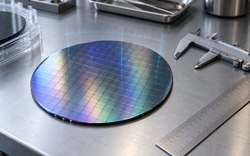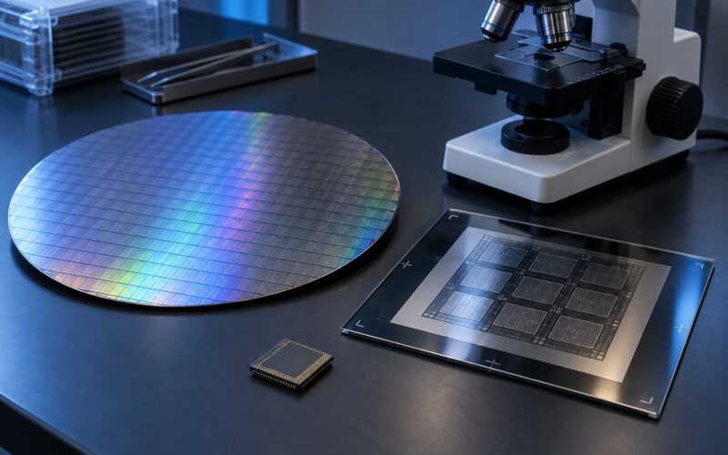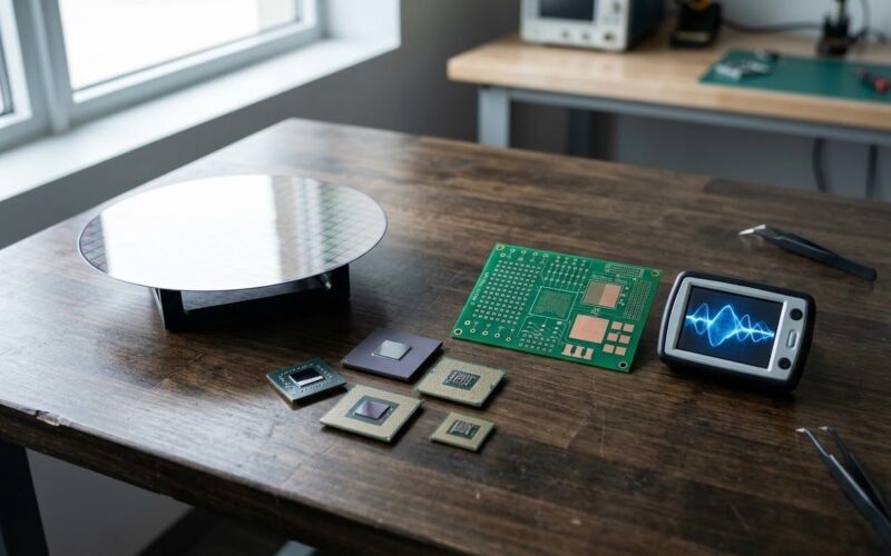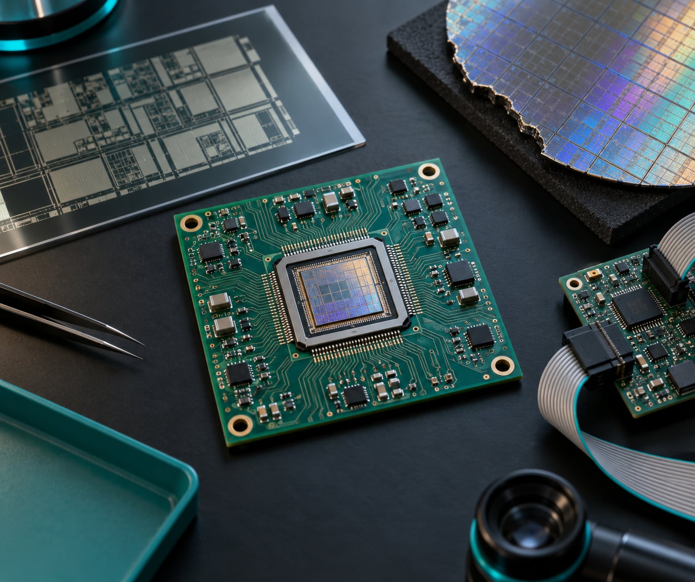
Tiny tapeout program explained in one line: it is an open-source shuttle service that lets students, hobbyists and independent engineers reserve a tiny block of area — a tile — on a shared test chip, and get that design fabricated as real silicon alongside hundreds of strangers’ projects. The cost of a mask set gets split across every participant, which is the whole trick.
That framing matters, because a conventional tapeout at the same process node needs a full mask set before a single part exists, and that mask set is what makes it out of reach. This guide walks through what the program is, how a submission travels from an empty repository to a packaged chip, what the constraints really are, and where the limits bite.
Table of Contents
- What Is a Tiny Tapeout Program?
- Why is it called tapeout?
- What is tapeout in IC design?
- How Does a Tiny Tapeout Program Work?
- The Tiny Tapeout Program Explained: One Wafer, Hundreds of Designs
- What Kind of Chip Can You Build?
- How Are Multiple Designs Put on One Wafer?
- What Files and Tools Does the Project Require?
- What common build failures actually mean
- What Is the Difference Between Tiny Tapeout and a Normal Tapeout?
- Which submission template should you use?
- How Much Does a Tiny Tapeout Cost?
- What Are the Main Design and Process Constraints?
- Which process should you target?
- Who should skip this entirely?
- What Happens During Fabrication and Bring-Up?
- How Can You Increase the Chance of Success?
- Frequently Asked Questions
- Do I need advanced IC design experience to join a tiny tapeout program?
- Can I use a tiny tapeout design in a commercial product?
- Will my tiny tapeout chips be packaged automatically?
- How many transistors or gates can fit in a tiny tapeout design?
- What should I verify before submitting my design to the shuttle?
- Key Takeaways and Next Steps
What Is a Tiny Tapeout Program?
A tiny tapeout program is an open-source silicon shuttle program where many unrelated chip designs share one wafer fabrication run. Each participant buys a small slice of the die area, gets their own documentation slot in the shuttle datasheet, and receives their die mounted on a small breakout board. Everyone pays a fraction of what a dedicated mask set costs.
- Shared mask set. One set of masks serves every design on the shuttle, so the mask cost divides across all of them.
- Open-source process. Shuttles run on published PDKs such as SkyWater sky130, IHP SG13G2 and GlobalFoundries GF180, with open-source EDA tools doing synthesis, place and route and GDS export.
- Bounded design area. You design into a tile, roughly 160 by 100 micrometres, with a fixed pin budget around it.
Why is it called tapeout?
Tapeout is the moment a finished design is released for manufacturing, and the name comes from the mask-making process itself: photolithography equipment writes each layer of the chip onto a photographic mask, historically delivered as tape, and the factory needs the complete set of masks before it can print any wafer. Nothing about the word is small. Tiny tapeout borrows the name for the milestone, not for the size.
Once the masks ship, the cost is committed. Everything after that point is manufacturing variation, not design changes, which is why tapeout is treated as a deadline rather than a milestone you can revisit.
What is tapeout in IC design?
In integrated circuit design, tapeout is the release of a verified, placed-and-routed layout — normally a GDSII file — to a foundry for mask generation and wafer fabrication. Before tapeout, a design can still be edited. After it, the only fixes are metal-only respins or a whole new tapeout. A shuttle does not remove that discipline; it just lowers the price of the commitment.
People use three terms as if they were interchangeable, and they are not. Getting them straight saves a lot of confusion in forum threads and older tutorials.
| Term | What it actually means |
|---|---|
| Mask set | The full set of photolithography masks, one per drawn layer. The dominant cost in any tapeout. |
| Tapeout | The milestone of releasing a finished design for mask generation and fabrication. |
| MPW | Multi-project wafer: one wafer run split among several customers’ designs, usually with each party paying an area-based share of the masks. |
| Shuttle | The MPW’s institutional form. One shuttle ASIC design, one deadline, many participants, usually open-source tooling and open PDKs. |
| Tile | The fixed slice of die area inside the shuttle ASIC that one participant designs into. |
| Die | One fabricated, separated piece of silicon. On a shuttle it carries a single participant’s tile. |
| Devkit | The board pair carrying that die — a breakout board plus a demo board driven by a host microcontroller. |
| PDK | Process design kit: the rulebook for a process, containing the standard cell library, device models and design rules. |
A shuttle is a specific, open, community-run flavour of MPW, and a tiny tapeout program is the participant-facing service that sells you a slot in one. The technical deadline is the same event in every case.
How Does a Tiny Tapeout Program Work?
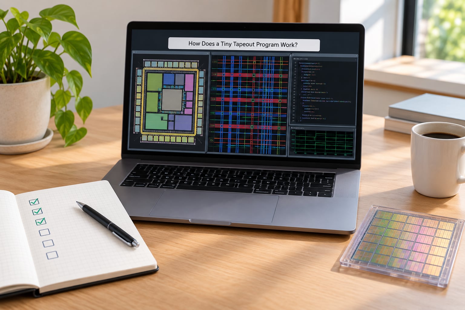
The sequence is fixed and it runs on someone else’s calendar, not yours. Shuttle deadlines are absolute — miss one and you wait for the next run.
- Pick an open shuttle. Choose from the published shuttle calendar by process, tile availability and deadline. IHP SG13G2 shuttles tend to be the common entry point, and some runs include analog slots alongside the digital tiles.
- Fork the matching template. Templates exist for the Wokwi visual builder, for Verilog or SystemVerilog flows, and for analog blocks. The template ships with the CI already wired for that shuttle’s PDK.
- Describe your design in
info.yaml. You set the source file list, the top module name and your documentation fields. Getting this file wrong is the most common reason a submission never builds. - Push and let CI build it. A GitHub Action runs synthesis, place and route, DRC and GDS export, then renders a results page with the GDS viewer and the reports you need to read.
- Verify before the deadline. Simulate, prototype on FPGA if your design is sequential, and read the report. Design that fails DRC does not reach the wafer.
- Submit. You merge a submission commit, pay the fee for your slot before the cut-off, and your design is locked into the shuttle.
- Wait for fabrication. The shuttle closes, the masks are made, the wafer is processed and the design gets an entry in the shuttle datasheet.
- Receive your devkit. You get your die on a breakout board, plus a demo board that drives it from a host microcontroller so you can see it work without a lab bench.
The Tiny Tapeout Program Explained: One Wafer, Hundreds of Designs
Here is the economics in plain terms. A conventional 180nm tapeout needs a full mask set, and a full mask set is the expensive part — the wafers that follow are comparatively cheap. A shuttle buys one mask set for everyone, then repeats the entire design flow once per participant tile. Because masks dominate, splitting that cost two hundred ways turns an impossible number into a personal one. The tiny tapeout program explained simply: you are not paying for a chip factory, you are paying your share of one shared mask set.
The catch is that every participant inherits the shuttle’s process, its area budget and its schedule. You get a fraction of a real flow, not a private one.
What Kind of Chip Can You Build?
Anything that fits the tile and respects the pin budget is fair game. Popular builds include seven-segment counters, blinkers, serial shift-register displays, small state machines, simple cipher engines, ALU and instruction-decoder experiments, and recreations of classic processor subsets.
For students, a counter with a readable waveform beats an ambitious core every time. The design fits, it verifies, and you learn the whole flow end to end.
For analog work, some shuttles offer analog slots at 1×2 or 2×2 tile size, where you can put a bandgap reference, an op-amp front end or a sensor amplifier through the real process. Those slots are priced separately from a digital tile and are allocated on a different basis.
What does not fit is worth stating plainly. Off-chip memory interfaces, high-speed serial links, USB, DDR and anything needing fine analog accuracy across a wide range are out of reach at this pin count and area. So is anything needing volume, since the shuttle produces a handful of your dies, not a production quantity.
How Are Multiple Designs Put on One Wafer?
The shuttle ASIC is one fixed design created long before you arrive. It contains a rectangular array of user tiles, and every participant’s tile is placed into a slot in that grid at build time.
Around the grid sits the infrastructure that makes an otherwise disconnected block testable: a pad ring that brings power, ground, clock and reset to every tile; the GPIO pads that route your pins to the outside world; and guard structures between tiles to limit crosstalk and provide well and substrate tie points. The top-level logic muxes the selected tile’s signals onto the shared pads.
Each submitted design is legalised into its tile rather than placed freely, which is a different constraint from a commercial flow. The flow will trim, buffer and sometimes resize cells to make your logic fit, and it can fail outright if it does not fit. When two designs share a neighbour, they share nothing functional — no clock, no state, no bus. Coexistence is purely physical.
What Files and Tools Does the Project Require?
A submission repository is small on purpose. The core files are your HDL sources under a src/ directory, your info.yaml metadata file, and the documentation fields the shuttle datasheet publishes — author, title, description, how it works, how to test, and language.
Around that sit the supporting pieces: a testbench or simulation harness to prove the design works, a constraints file for pin assignment and timing, and the shuttle’s build configuration, which carries the PDK version and target frequency.
The toolchain runs in CI so you do not install anything locally. Synthesis is done by Yosys. Place and route, DRC and GDS export come from LibreLane with OpenROAD doing the physical work. The result is a GDSII file plus a build report. That is the open-source ASIC flow in miniature, and running it against a real process is the actual educational payload of the program.
One practical note: the same template builds against one PDK only. Hardening a design for sky130 and submitting it to an IHP shuttle produces a PDK mismatch error, not a silent failure.
What common build failures actually mean
Most first submissions do not fail because the design was too clever. They fail on configuration, and the error text usually points straight at the fix.
| Symptom | What it means | Fix |
|---|---|---|
| PDK mismatch error | Design hardened against a different process than the shuttle | Use the template matching your shuttle; do not mix flows |
| CI action never runs | GitHub Actions not enabled on the fork | Enable Actions in the repository settings |
| Results page is blank | Pages configured to serve from a branch or folder that is not built | Point Pages at the branch and folder the action populates |
| Unmapped cell warning | A flip-flop or cell the standard library does not recognise | Map it or replace it with a supported primitive |
| Design will not fit | Legalisation cannot fit the logic inside the tile | Shrink the design, or buy a larger tile option |
| GDS export very slow | Design is oversized for its tile | Treat as a sizing signal and trim scope |
None of these are hardware faults, and all of them are visible before the deadline if you actually open the build report rather than trusting a green tick.
What Is the Difference Between Tiny Tapeout and a Normal Tapeout?
| Factor | Tiny tapeout shuttle | Conventional tapeout |
|---|---|---|
| Wafer quantity | One shared wafer per shuttle | Typically hundreds to thousands |
| Cost model | Share of one mask set plus processing | Full mask set plus NRE plus processing |
| Design area | One tile, roughly 160 by 100 micrometres | Whatever the project needs |
| Intent | Learning, prototyping, open-source projects | Production, commercial shipment |
| Turnaround | Roughly six to nine months to silicon | Weeks to a few months for the first wafers |
| Engineering support | Community Discord, office hours, documentation | Paid foundry and design house support |
| Volume suitability | Not suitable for commercial quantity | Built for it |
| Pin budget | About 24 general-purpose I/O | Set by the die and package |
The honest reading is that a shuttle is not a cheap substitute for production. It is a cheap way to learn the production flow on real silicon, which is a much rarer thing than it sounds.
Which submission template should you use?
| Template | Skill needed | Best for | Trade-off |
|---|---|---|---|
| Wokwi | None | First-time submitters, teaching labs, quick blinkers | Limited to what the builder models |
| Verilog / SystemVerilog | RTL fundamentals | Processors, pipelines, anything sequential | You own the architecture and verification |
| Chisel or VHDL templates | Language-specific experience | People coming from those ecosystems | Build flow needs extra setup |
| Analog slot | Analog design fundamentals | Bandgaps, amplifiers, sensor front ends | Separate allocation and pricing rules |
Most first submissions should be Wokwi or a small Verilog module. The gate budget is real, and a design that does not route is a wasted deadline.
How Much Does a Tiny Tapeout Cost?
The final fee is set per shuttle, not per program, and it moves with the run you join. Rather than quote a figure that will be stale the moment you read it, here is what actually drives the number, so you can predict your own.
| Driver | What it changes |
|---|---|
| Shuttle chosen | Base fee varies by process, area and provider |
| Tile count | Extra tiles are a flat per-tile add-on; you pay before you know whether you need them |
| Pin options | Additional analog pins and special pad assignments add cost |
| Analog slot | Priced and allocated differently from digital tiles |
| Early bird window | A discounted tier that usually closes before the deadline |
| Timing | Late submissions may have fewer tile options |
| Destination country | Postage is quoted separately and varies by destination |
Treat these as planning bands, not quotes. The authoritative number lives in the official pricing calculator on the shuttle page for the run you intend to join, and it is the only figure worth committing a budget against. Community discussions around these shuttles show the same pattern: people who check the calculator before starting commit without hesitation, and people who guess are the ones who get surprised.
For context on why the model is so much cheaper, a full-mask tapeout at a comparable mature node has historically run into six figures for masks and engineering costs alone. That gap, not convenience, is the reason the shuttle exists.
What Are the Main Design and Process Constraints?
Tile area is the binding constraint, and it is less intuitive than the gate number suggests. A commenter in a Hacker News thread on the program calculated the tile area and still could not reconcile a die area four times larger with a four-tile requirement. Density rules are part of why: standard-cell flows target roughly 60 percent utilization, because tap cells and antenna diodes need room and the remaining area is deliberately left open.
- Area. One tile is roughly 160 by 100 micrometres, so a 1×2 or 2×2 purchase multiplies the budget. A recurring community estimate is around a thousand gates in a single tile, far less than the gate count alone suggests once buffers and fillers are counted.
- Pins. Roughly 24 general-purpose I/O split into inputs, outputs and bidirectional pins. Budget pins before gates — a design that needs a memory bus will not fit the interface, no matter how small the logic is.
- Process. Supported PDKs have included sky130, IHP SG13G2 and GF180. Each is a mature node, roughly Pentium III to IV era capability, which is deliberate: mature nodes have open PDKs, cheap masks and forgiving design rules.
- Density. The flow targets about 60 percent so tap and antenna cells fit. Designs that assume full utilization fail.
- Clock. Designs are expected to close at 50 MHz or above, with a dual-clock recipe documented for designs needing more than one domain.
- Verification. DRC and LVS must pass. There is no engineering support to debug a silicon bug afterwards.
One practical early warning: if the GDS export step in CI suddenly takes far longer than a couple of minutes, the design is probably too large for its tile. That runtime is a useful sizing signal long before a human looks at the report.
Which process should you target?
| Process | Node | Character | Good fit for |
|---|---|---|---|
| sky130 | 130nm | Mature open PDK, well documented cell library | General digital designs and first-time submitters |
| IHP SG13G2 | 130nm class | Widely used shuttle process with the largest run history | Verilog flows and repeat submitters |
| GF180 | 180nm | Very forgiving rules, tolerant of rough designs | First-time builders and larger analog slots |
All of these are mature nodes, and that is a feature rather than a limitation. Open PDKs, cheap masks and forgiving rules are exactly what makes a shared shuttle viable. What you give up is density and switching speed, so a design that would be routine at a leading-edge node simply does not fit.
Who should skip this entirely?
Some projects are a poor fit and it is worth saying so directly. Anything requiring DDR, high-speed serial links or USB is out, because the pin budget and timing close on offer will not carry it. Anything needing commercial volume or an implied temperature range is out, because a shuttle produces a handful of dies with no qualification behind them. Anything needing vendor support after fabrication is out, because the help stops at the deadline.
If your project needs any of those, use the shuttle to de-risk a digital block, then move to a commercial shuttle or a full tapeout once the architecture is proven.
What Happens During Fabrication and Bring-Up?
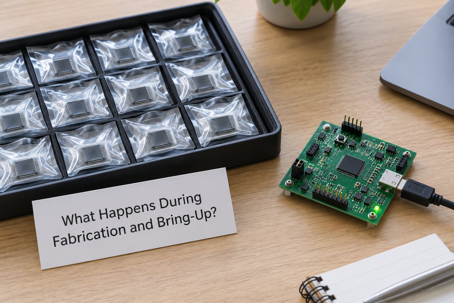
After the deadline, the shuttle closes and the work becomes invisible for months. The shuttle design is checked out, the combined GDS goes to the fab, masks are generated, and one wafer carrying every participant’s tile is processed. The shuttle is then diced, dies are packaged or mounted, boards are assembled, tested, and handed to a fulfilment step.
| Stage | What happens | Who controls it |
|---|---|---|
| Submission window | Designs merged, fee paid, tile allocated | You |
| Deadline | Shuttle closes and the ASIC is locked | Program |
| Integration and checkout | Your tile is placed in the grid and the full design is checked | Program |
| Mask generation | One shared mask set written from the combined GDS | Fab |
| Wafer fabrication | Every participant’s tile is processed on one wafer | Fab |
| Dicing and packaging | Dies separated and mounted or packaged | Assembly partner |
| Board assembly and test | Breakout and demo boards assembled and tested | Assembly partner |
| Fulfillment | Address collected, devkits dispatched to you | Program |
Roughly six to nine months from deadline to silicon is normal, and the fuller end of that range accounts for assembly and testing. Your delivery address is collected after manufacture, not at checkout, so keep an eye on the confirmation email when the run closes.
Your devkit arrives as two boards. The breakout board carries your die and fans the pins out to headers; the demo board hosts an RP2040-class microcontroller that drives the die through a defined set of signals, so a design that passes verification usually shows visible behaviour as soon as you plug it into USB.
When a chip misbehaves, the information available is thin. You have the datasheet, your own simulation and FPGA results, and the GDS viewer. There is no probe on the fabricated die and no engineer on call, so bring-up is closer to a hardware debugging session than to a support ticket.
How Can You Increase the Chance of Success?
Start with the official example for your shuttle and submit it unchanged once. That single step teaches you the repository layout, the CI behaviour and what a passing build report looks like, and it costs one deadline rather than your only shot at a first design.
Then work through the checks that catch most failures:
- Simulate the design before touching the layout, and run lint early so naming or width mismatches surface in seconds rather than in the build.
- Prototype on FPGA if your design is sequential. It is far cheaper to find a state machine bug there than on silicon.
- Read the DRC and the build report every time. A design that routes but reports issues may still be printed differently than you expect.
- Budget pins first. Count what you need to reach the outside world, then work out what logic fits in the remaining budget.
- Check the GDS viewer early and often, not just at the end, so you catch a tile overflow while it is cheap to change.
- Preserve power, ground, clock and reset paths. Designs that get unstable on the first power-up usually had a marginal supply or reset path.
- Use the community Discord and office hours before the deadline rather than after. Design review is the one support channel that actually exists.
If you follow an older tutorial, check where it points. The platform this program originally ran on shut down in March 2025, and the ecosystem moved to wafer.space shuttles. Plenty of 2023 and 2024 walkthroughs still send you to a dead platform.
Frequently Asked Questions
Do I need advanced IC design experience to join a tiny tapeout program?
No. The Wokwi template lets you draw a circuit in the browser and submit it with no RTL experience, and many first-time submitters report getting a working design through the flow in an evening or two of effort. Hardware description languages give you more control but are not a prerequisite. What you do need is willingness to read the build report, because nobody is debugging the design for you once it is fabricated.
Can I use a tiny tapeout design in a commercial product?
You own your design and can license it under the terms you chose for your repository, but the hardware is not a commercial route. A shuttle yields a handful of dies and no volume path, so it is unsuitable for a shipping product. Treat the shuttle as a prototype that de-risks an idea, then move the verified design into a commercial shuttle or a proper tapeout when the economics justify it.
Will my tiny tapeout chips be packaged automatically?
Packaging depends on the shuttle, and this is worth checking before you commit. Depending on the run, your die may arrive mounted chip-on-board on a breakout PCB, or in a conventional package on a small assembled board. Either way the devkit pairing means you can plug it into a host microcontroller and see it run. Confirm the packaging method on the shuttle page for your specific run, since it varies.
How many transistors or gates can fit in a tiny tapeout design?
A single tile is roughly 160 by 100 micrometres, and community estimates land around a thousand gates of mixed logic before buffers and fillers. The raw gate figure is misleading because the flow targets about 60 percent utilization to leave room for tap and antenna cells. Larger designs buy extra tiles, which multiply the area and the fee, so budget the tile before committing to an architecture.
What should I verify before submitting my design to the shuttle?
Simulate the design and confirm the timing closes, then prototype on FPGA if it contains sequential logic. Run the full CI build and read the DRC and LVS results, open the GDS view and confirm your logic fits inside the tile. Check that your PDK matches the shuttle, because a sky130 design submitted to an IHP run fails outright. If the GDS export suddenly takes much longer, treat that as a sign the design is oversized.
Key Takeaways and Next Steps
If you want to start now: identify the open shuttle with the next deadline, read its supported process and tile dimensions, clone the official example and submit that first, then build your own design against a verified template. Budget pins before logic, simulate before layout, and treat the CI report as the source of truth rather than a formality.
That is the tiny tapeout program explained in practical terms — a shared mask set, a bounded tile, an open-source flow and a six-to-nine-month wait, in exchange for a real chip you can hold. Everything else is detail on top of that trade.