Clock gating stops a clock from toggling into logic that has nothing to do, which removes dynamic power but keeps the block powered. Power gating disconnects the supply rail to an idle block with header or footer transistors, which removes leakage as well. The first is cheap and instant to wake; the second is expensive and takes microseconds to restore. That one difference drives most low-power design decisions on a modern chip.
This guide is written for RTL designers, synthesis and physical design engineers, and verification leads who already know synchronous digital design and now need the low-power picture in one place. It assumes you can read a Verilog always block and a timing report, but it does not assume EDA tool experience.
Table of Contents
- Clock Gating and Power Gating Explained
- Clock Gating vs Power Gating
- How Clock Gating Reduces Dynamic Power
- How Clock Gating Works in RTL and Synthesis
- How Power Gating Reduces Leakage and Active Power
- Where Clock Gating and Power Gating Are Used
- Benefits, Tradeoffs, and Design Pitfalls
- How to Verify and Implement Low-Power Features
- Frequently Asked Questions
- Is clock gating the same as power gating?
- What is the main difference between dynamic and leakage power?
- Does clock gating affect a design’s functional behavior?
- When should a design use power gating instead of clock gating?
- How do designers verify clock gating and power gating?
- Conclusion
Clock Gating and Power Gating Explained
A clock in VLSI is the periodic signal that advances every register in a synchronous design on the same edge. Because every flip-flop in the design is wired to that one timing network, the clock toggles on every single cycle whether or not the data behind those flops is changing. That is the waste both gating techniques exist to remove.
Total chip power splits into two very different terms:
P_total = alpha * C * V^2 * f  +  I_leak * VDD
            _______________/     ___________/
              dynamic (switching)      leakage (static)
Dynamic power is charged every time a node with capacitance C flips at frequency f, scaled by the activity factor alpha and the square of the supply voltage. Leakage is the current that flows through every transistor whether it is switching or not. At advanced nodes, subthreshold leakage has grown large enough that it can match or exceed the dynamic term during idle periods.
Clock gating attacks the first term. Stop the toggles and alpha for that block collapses toward zero. Power gating attacks both: once the supply is physically disconnected, the transistors in that block have no VDD across them, so neither switching nor subthreshold current can flow through them.
The scale of the clock problem explains why clock gating is in every modern flow. Clock tree and clock circuitry together account for roughly 15-45% of total chip power, depending on the design and how the number was measured. Sources in the literature and industry presentations cluster in that band, and the exact figure swings with datapath width, register count, fanout, and the voltage and frequency the design runs at. A datapath-heavy accelerator usually sits at the low end of that range. A wide register file sitting at a high DVFS operating point sits at the high end.
Which technique to reach for follows from how long the block stays idle. A block that goes quiet for tens or hundreds of nanoseconds and then comes straight back is a clock gating candidate, because a gated clock resumes on the next edge. A block that sits unused for milliseconds or for an entire standby session is a power gating candidate, because leakage drains for that whole window whether or not the clock is running.
Clock Gating vs Power Gating
The two techniques differ on almost every axis that matters to a design team. The table below is the version I keep open while reviewing power intent files.
| Criterion | Clock gating | Power gating |
|---|---|---|
| What it disconnects | The clock path feeding a register bank | The supply rail feeding a whole power domain |
| Power removed | Dynamic (switching) power of that block, plus clock tree switching | Leakage and dynamic power of the entire domain |
| State when inactive | Fully preserved; registers hold their values | Lost unless retention flip-flops or a save path is used |
| Wake-up latency | Zero; ready on the next active clock edge | Typically 1 to 100 microseconds depending on rail and isolation design |
| Typical savings | Roughly 20-40% of total dynamic power | Roughly 80-95% of a block’s power while in sleep |
| Area cost | About 5-10% overhead from ICG cells | About 20-40% extra area on retention flops and library overhead |
| Implementation artifact | ICG cell in the capture clock path | Header PMOS or footer NMOS plus VVDD/VGND virtual rails |
| Granularity | Fine: a single register bank, datapath unit, or clock root | Coarse: an entire domain, sometimes with sub-switchable regions |
| Primary failure mode | Glitch on the enable passes through and clocks registers wrongly | Retention failure, isolation or reset race, unisolated X propagation |
| Verification burden | Enable timing checks, glitch analysis, gate-level simulation | Power state table coverage, isolation and reset sequencing, rail stability checks |
| Best use case | Short idle gaps, unused multiplier or FPU, register file read mode | Standby and deep sleep, switchable accelerator island, long idle stretches |
| Usually owned by | RTL and synthesis, with CTS reviewing the gated clock | Physical design and low-power verification, with RTL declaring intent |
One clarification worth making early, because the same word gets used for three different things. Clock gating stops a clock. Power gating removes a supply. Data gating holds combinational output steady when the register bank behind it is idle. Only the first two are about power domains and power intent, and only the first two are what this article covers.
There is also a narrower comparison inside power gating itself, which is the switch topology choice:
| Aspect | Header switch (PMOS) | Footer switch (NMOS) |
|---|---|---|
| Rail switched | VDD, supplying VVDD to the domain | VSS, returning VGND from the domain |
| Leakage path in off state | Subthreshold through the PMOS itself | Stacked transistors reduce off-state leakage |
| Wake-up behaviour | Faster; the rail ramps from the top | Slower; the rail ramps from the bottom |
| Area overhead | Smaller device for the same resistance | Larger device to carry the same current |
| Typical use | Standby domains needing quick resume | Deeper off-state isolation where leakage matters most |
How Clock Gating Reduces Dynamic Power
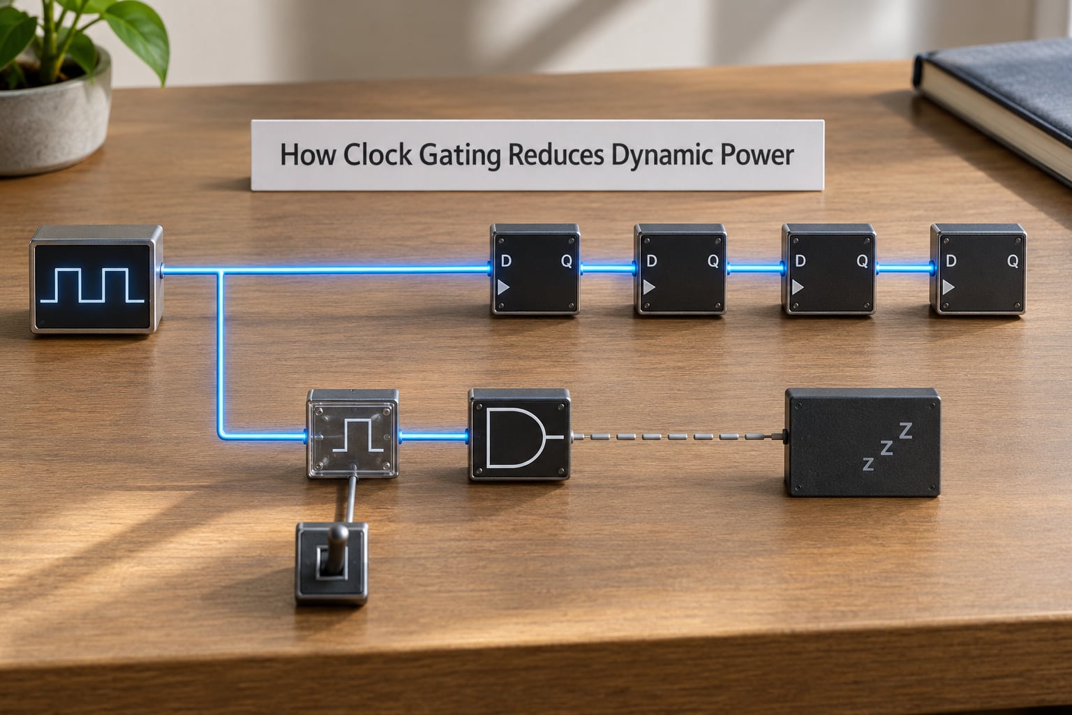
Every time a node switches, the driver has to charge the parasitic capacitance hanging off that net, and the discharge current has to come back through the driver. Charge drawn from the supply per transition is proportional to C times V, so the energy per transition is C times V squared. Do that at every clock edge across every register bank, and you get P = alpha * C * V^2 * f.
The important consequence is that energy follows toggling, not data. A pipeline register that reads the same value every cycle still burns switching power every cycle, because the clock edge drives its internal nodes regardless. Gating the clock on an enable signal makes alpha for that bank collapse to the fraction of cycles where data actually changes, typically a small number.
There is a second, less obvious saving. Backend engineers point out that clock gating stops switching in the clock tree buffers feeding the gated bank as well as in the leaf flip-flops themselves. A gate deep in the tree that stops toggling upstream of it removes the buffer chain activity too, which is why coarse gating at a clock root can save more than the arithmetic on the flop bank suggests.
Here is the catch that the definition hides. A flip-flop with no clock edge does not update. If you gate a bank that was supposed to capture new data on that edge, the register keeps its old value and your functional result changes. Clock gating is safe only when the enable is provably aligned with the data you intend to capture. That is the entire argument for the ICG cell described in the next section, and it is also the source of the practitioner objection that gated clocks are risky.
The objection is fair for raw gated clocks. A hand-built AND gate in front of a clock net will happily pass a glitch on the enable straight through to the flops, and a combinational gate has no memory of when the enable changed. Practitioners on engineering forums say this plainly: many teams prefer a clock enable into a muxed D input instead of gating the clock, because the mux keeps a real clock edge on every flops while the data simply holds.
Both approaches are legitimate and they are not equivalent. A clock enable costs a mux in front of every flop data pin, so its area scales with the number of registers and it adds a mux delay to the data path. A gated clock costs one ICG cell per bank and no data-path delay, which is why clock gating wins on datapath-heavy logic. The counter-argument for the enable style is that it leaves the clock tree intact and avoids any question of a new clock existing in the netlist. Choose per block: gating for wide datapaths, enable for narrow control logic where the mux is cheap.
How Clock Gating Works in RTL and Synthesis
The standard implementation is the integrated clock gating cell, usually called an ICG. It is a negative-level-sensitive latch feeding an AND gate, and the latch is the part that matters.
        EN      +---------+
  +-----------| D     Q  |--- CK
  |           |  latch  |     |
  |           +---------+     |   +-----+
  |            transparent     +---| AND |---- ECK (gated clock)
  |            when CK = 0     |   +-----+
  |                                  |
  |                              +-------+
  +------------------------------|   CK  |
                                 +-------+
During the low phase of the clock, the latch is transparent and EN passes straight through to the AND input. During the high phase the latch closes and holds whatever EN was at the falling edge. The AND output therefore can only begin to change while the latch is transparent, so the gated clock can never produce a narrow pulse inside the high phase. A glitch on EN that happens while CK is low gets passed, but by then the AND output is being driven toward the same value it will settle at anyway. A glitch that happens while CK is high is blocked by the closed latch.
That is the whole argument for a latch instead of a flip-flop. A flip-flop samples only on an edge, so between edges its output can change for any reason and the glitch gets straight through to the clock net. The latch is level-sensitive and transparent for the entire safe half of the cycle.
The cost of the latch is timing: EN must be stable a setup time before the clock’s rising edge and hold time after it, because the value sampled during the low phase is what determines the whole high phase. STA tools report these as enable setup and enable hold checks on the ICG input. Skipping those checks is a classic sign-off gap, because everything else in the design looks clean.
Writing RTL that infers an ICG is mostly about coding style. Synthesis infers gating when an enable is applied consistently to every register in a group through the clocked block:
// Infers an ICG cell on the clock, plus operand isolation on the D pins
always_ff @(posedge clk or negedge rst_n) begin
  if (!rst_n) begin
    q1 <= 8'h00;
    q2 <= 8'h00;
  end else if (en) begin
    q1 <= next1;
    q2 <= next2;
  end
end
Note that en is used in both flops in the same always block with no conflicting condition elsewhere. That consistency is the trigger. A style that produces a mux on the data path instead:
// Produces a data mux, not an ICG, because the enable never reaches the clock
always_ff @(posedge clk or negedge rst_n) begin
  if (!rst_n)       q1 <= 8'h00;
  else if (en_sel)  q1 <= in_a;
  else              q1 <= in_b;
end
Designers force the issue with pragmas and constraints when the coding style is ambiguous. Synopsys Design Compiler and Cadence Genus both take set_clock_gating_style style arguments covering latch-based gating, the positive or negative polarity of the enable, and whether to gate at the root or at the leaf. In the UPF portion of the power intent file, the same intent is expressed as a clock gating style plus the set_port_attributes and enable rules that the implementation tools read.
Two modes always need thought. In scan or test mode, the clock to a gated bank may be required to toggle even when the functional enable is low, so a test enable has to be ORed into the ICG enable path. That bypass has to be invisible in normal operation, and its timing is a common source of ECOs late in the schedule. Separately, if the enable for a bank comes from a different clock domain, you need proper synchronisation on that enable; gating across an unsynchronised boundary is a metastability path that no tool will stop you from creating.
Two related terms come up often enough to be worth pinning down. Clock gating granularity refers to how much logic sits behind one ICG: leaf gating covers a single register bank, root gating covers a whole subsystem, and hierarchies in between are common. And when people list the types of clock gating, they usually mean AND-based gating on an active-high enable, OR-based gating on an active-low enable, ICG-based latch gating, data gating, and manually inserted gating in RTL. Only the ICG form is safe against enable glitches without extra care.
For completeness, the broader clock distribution question usually gets answered like this. A clock tree is built as an H-tree or a balanced buffer tree from the root, buffers are inserted for fanout and skew, root gating cuts whole subtrees, leaf gating cuts individual register banks through ICG cells, and gated clocks are then treated as ordinary clock nets by CTS. Skew, insertion delay, and useful skew all matter here, which is why gating decisions are reviewed by both the RTL owner and the CTS engineer.
How Power Gating Reduces Leakage and Active Power
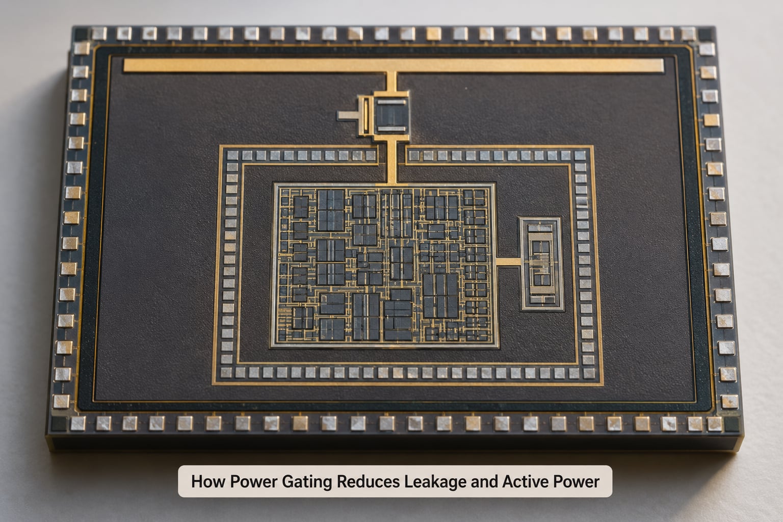
Power gating puts a controllable transistor between the main rail and the block, and drives that transistor from a software-managed sleep signal. In a header topology the device is a PMOS in the VDD path and the block runs off a virtual supply called VVDD. In a footer topology the device is an NMOS in the VSS path and the block runs off a virtual ground called VGND. In both cases the physical rail stays connected to the pad; only the internal connection to the block is broken.
The saving is straightforward. With the header off, the block’s transistors have no supply across them, so subthreshold current through them stops and the leakage term of the power equation drops to nearly zero. Active power is already near zero in an idle block, and now the residual dynamic power from glitching internal nodes disappears too. Measured on real blocks, that lands in the 80-95% range of the block’s total power over a long sleep window.
The reason power gating is harder than clock gating is that you are now changing the electrical environment of a block, not just one signal. Three classes of cell have to be inserted at the domain boundary to keep the rest of the design intact.
Retention flip-flops, also called balloon latches, sit inside the powered-down domain and hold the handful of architectural registers that must survive. Before the rail is cut, a save control copies the value into an always-on cell; after power returns, a restore control copies it back. Sizing is a real design decision: retain only the state that software or hardware will actually check on wake-up, because each retained flop can add 20-40% area across a wide bank.
Isolation cells clamp every signal leaving the powered-down domain to a known value while the rail is off. Without them, the outputs of unpowered flops are undefined and propagate X or garbage into the always-on side, where it lands in control FSMs and ends up as a mysterious reset. The clamp value is chosen deliberately: hold the signal at its inactive value so downstream logic sees a block that is simply idle.
Level shifters sit alongside the isolation cells wherever two voltage domains meet. They are not strictly about gating, but any domain boundary needs them, and power-gated domains are where most new ones get introduced.
The power-down and wake-up sequences are the part most likely to be wrong. Powering down, in order: assert isolation, wait for isolation to take effect, assert the retention save and wait for it, assert the switch control, then wait for the rail to collapse before releasing anything further. Waking up runs the reverse: assert the switch control, wait for a power-good flag confirming the rail is stable, de-assert the retention save so state is restored, de-assert isolation, then release reset to the block.
Two physical effects make that wait non-optional. The rail has an RC time constant, so it does not reach voltage instantly, and starting to clock a domain on a sagging rail produces timing failures that look like logic bugs. And re-energising thousands of transistors at once is an inrush current event: the switch is effectively a short across a large capacitor bank, so current spikes and the rail dips. That dip is IR drop, it scales with how fast you switch, and it is why switch sizing is a power integrity decision rather than a logic decision. Switches that are too large create IR drop; switches that are too small make wake-up slow and add series resistance to the active path, which shows up as delay.
That last point is the practical caveat engineers quote most often: power gating is generally applied in standby to cut static power, but it increases the delay of the cells in that block because of the extra resistance and the body effect from the header or footer device. A block that must hit full frequency immediately after wake-up can be hurt by the very switch that saved its power.
The design intent itself is written in UPF, the IEEE 1801 standard. A minimal version creates the domain, the switch, the retention and the isolation rules, and the power state table:
create_power_domain PD_ACC -elements {u_acc}
create_power_switch PS_ACC -domain PD_ACC \
  -input_supply_port {VDD} -output_supply_port {VVDD_ACC} \
  -control_port {sleep_n} -on_state {ON VDD {sleep_n}}
set_isolation ISO_ACC -domain PD_ACC \
  -applies_to outputs -clamp_value 0 -location parent
set_retention RET_ACC -domain PD_ACC -retention_supply_set VDD
create_pst PST_SOC -supplies {VDD VVDD_ACC} \
  -domain_elements {PD_ACC} -state {ON_SLEEP -logic {ON 0 <=sleep_n 1}}
The power state table is the piece that matters most and that gets the least review. It is the formal definition of which combination of supply states and signals is legal. If a state a testbench can reach is missing from the table, the design will produce X in simulation and undefined behaviour in silicon, and the gap will not show up in gate-level simulation if your testbench never happened to generate that combination.
Where Clock Gating and Power Gating Are Used
Processors use both, at different scales. Inside a CPU core, clock gating sits on unused execution units: a multiplier or floating-point unit with no operation pending has its clock cut for tens of nanoseconds, and a register file that is only being read rather than written gates its write-side clock. Both wake instantly on the next cycle, which matters when a back-to-back instruction is waiting.
Outside the core, an always-on island handles interrupts, timers, and the real-time clock, and it is never power gated because something must always be running. Its leakage is accepted, and the tool used is usually aggressive multi-Vt assignment plus body bias rather than gating. Around that island, switchable domains hold the rest: a display controller, a wireless baseband, a neural accelerator, an unused camera pipeline. Those blocks are idle for long stretches of a phone’s life, so they get power gated, with retention on the handful of registers the power management controller needs on resume.
Caches are a good middle case. A cache line read in a design that stalls on it for hundreds of cycles is often clock gated during the stall because the block comes back quickly. A banked cache in a mobile part may be power gated per bank, with retention on the tags, when the application leaves the working set alone for a while.
Memory interfaces are mostly not gated directly, because a memory’s power is dominated by its own internals. What you gate is the controller and the datapath around it, and you put the interface into a low-power state protocol instead. On an accelerator, the pattern is similar: gate the clock on each compute tile’s enable, and power gate the whole accelerator island when no job is queued for hundreds of milliseconds.
Two worked cases show the contrast well. On a mobile part running an ARM Cortex-A series core, the DVFS operating point changes with load, so the core’s dynamic power is managed by frequency and voltage while the physical characteristics of power gating supply the always-on floor. On a data-centre accelerator, thermal limits are reached during active operation rather than at idle, so there the ordering flips: clock gating and operand isolation on the datapath come first because they reduce heat during work, and power gating of unused tiles comes second for the idle case.
Benefits, Tradeoffs, and Design Pitfalls
Clock gating buys a large dynamic power reduction for roughly 5-10% area overhead and no data-path delay. That is why practitioners call it the low-hanging fruit of power optimisation: cheap, well understood, universally adopted. It leaves leakage untouched, so a block that is clock gated for a millisecond still leaks for that whole millisecond. It also creates a new clock net in the netlist, which means CTS, DFT and STA all have to treat it as a first-class clock.
Power gating buys 80-95% of a block’s power over a long sleep and is the only technique that reaches leakage. It costs 20-40% extra area on retained registers, microseconds of wake-up, new verification obligations, and a delay penalty on every cell in the domain. It also constrains physical design: the domain needs its own power ring, the switch has to be sized against IR drop analysis, and the boundary needs room for isolation and level shifters.
The failure modes worth naming are specific rather than abstract.
A glitch on a gating enable passes straight through a raw AND or OR gate and produces a runt pulse on the clock net, clocking registers at the wrong time. Latch-based ICG cells prevent this by only allowing changes during the clock’s low phase, and glitch-free variants use a two-latch arrangement if you need the stronger guarantee. The related bug is a lost pulse, where the enable changes entirely within one cycle and the block never sees the edge it needed. That one is an RTL bug, not a gate bug.
Clock tree disturbance shows up differently: a gated clock at the root changes load on upstream buffers, which changes their delay, which shifts skew into neighbouring ungated paths. CTS reviews gate placement for this reason, and badly placed root gates can produce timing closure churn that has nothing to do with your RTL.
On the power gating side, retention failures mean state that should have survived came back wrong, usually because save and restore were asserted for too short a window. Power state races mean a domain is powered off while a transaction from the always-on side is still in flight, or the isolation release races the rail ramp. Unisolated domains propagate X into control logic, which usually presents as a reset that nobody wrote.
The most common objection to gating in general is the logic left behind. Operand isolation and the muxes on data paths cost area and can eat into the saving, particularly on small blocks where the control overhead is comparable to the load. The fix is ungating anything with a high duty cycle: a block that is active 90% of the time pays the overhead for very little benefit.
One context where the whole discussion changes is FPGAs. Classic clock gating is normally avoided, because routing a gated clock through general-purpose interconnect would force dedicated clock buffers through LUTs, and the programmable routing cannot guarantee the glitch-free timing that a real ICG cell provides. Instead the FPGA route is a clock enable pin on the slice, which stops the sequential elements without creating a new clock. Xilinx calls this Intelligent Clock Gating, and the ICG cell becomes part of the enable chain rather than the clock chain. Same power saving, completely different implementation.
How to Verify and Implement Low-Power Features
The work is ordered, and each stage catches failures the next one cannot.
Start with power intent in RTL, using UPF or the equivalent vendor constraints. Declare domains, switches, isolation rules, retention, and the power state table before synthesis, because these drive what the implementation tools are allowed to insert. Define every state your hardware can legally reach, even the ones you expect never to happen.
Then let synthesis infer. Check the inferred gate list rather than assuming: count the ICG cells, confirm they are latch-based and not AND gates, and confirm the enable timing checks exist in the timing report. Add explicit gating constraints where the coding style was ambiguous.
Run equivalence checking at the boundary. A gated-clock netlist is not structurally equivalent to the RTL in the way a plain register rewrite is, so use the tool’s gating-aware mode and check that each register sees the same functional sequence of edges. This is where an enable that was inferred as a data mux rather than an ICG gets caught.
Gate-level simulation is where state retention and X propagation surface. Run the power state table as directed sequences, not just the functional stimulus: for every legal state, power down, confirm the rail collapses, confirm the boundary clamps, then power up and confirm the restored state matches the saved state bit for bit. Add X-propagation checks on every signal crossing a domain boundary so an unisolated output is a hard failure rather than a mysterious reset later.
Formal checks fill the coverage gaps a testbench will not reach. Assertions on the power state table, on isolation ordering relative to the switch control, on retention save and restore windows, and on the power-good handshake are straightforward to write and catch the racy states you will never think to stimulate. Static checks that every domain’s isolation and level shifter strategy is present and consistent run over the whole design rather than a chosen scenario.
Sign-off is where the physical numbers come from. Dynamic power analysis on the gate-level netlist with realistic activity shows whether the gating you asked for actually reduced switching, and reveals blocks where the clock never stopped. Static power analysis on the post-layout netlist shows the leakage the power gates are removing. IR drop analysis on the wake-up transient checks that the switch is not sized so large that the rail collapses under inrush, and on-ramp checks the opposite case.
The named tools for this stage in a commercial flow are Ansys Redhawk or Cadence Voltus for dynamic power and IR drop, Synopsys PrimeTime for power-aware timing and leakage, and Cadence Innovus or Synopsys Fusion Compiler for the implementation and ECO work. Whatever the tool, the questions are the same: is the clock actually stopped in the block I expect, does the domain actually reach the off state, and does the rail come back fast enough.
Silicon validation closes the loop. Measure the rail current in each sleep state on a real part and compare it with the power report, because a switch that was not fully off, or a boundary that leaks through an unmodelled path, shows up only here. Correlation discrepancies of more than a modest fraction on a gated domain usually mean an unannotated path rather than a tool error.
Frequently Asked Questions
Is clock gating the same as power gating?
No. Clock gating stops the clock signal reaching a register bank, which removes dynamic power while the block stays powered and keeps its state. Power gating disconnects the supply rail through header PMOS or footer NMOS transistors, which removes leakage as well as dynamic power, at the cost of losing state unless retention is added. Clock gating wakes instantly; power gating takes microseconds.
What is the main difference between dynamic and leakage power?
Dynamic power is drawn only when a node switches, and scales with activity factor, capacitance, frequency, and the square of the supply voltage. Leakage power is drawn continuously through every transistor regardless of switching, and grows sharply at advanced nodes. Clock gating attacks dynamic power by stopping toggles. Power gating attacks leakage by removing the supply entirely from the block.
Does clock gating affect a design’s functional behavior?
It can, and that is the main risk. A gated register bank stops updating, so gating an enable that should have captured new data changes the result. A raw AND or OR gated clock also passes enable glitches straight through as runt pulses. Latch-based ICG cells prevent glitches, and correct inference plus enable setup and hold timing checks prevent the functional error.
When should a design use power gating instead of clock gating?
Use power gating when the block stays idle long enough that leakage dominates. Short idle gaps of tens or hundreds of nanoseconds suit clock gating because wake-up is instant. Idle windows of a millisecond or more, and any standby or deep sleep state, suit power gating. Retention, isolation, level shifters, sequencing, and IR drop checks all have to be built and verified for it.
How do designers verify clock gating and power gating?
Clock gating is checked with gate-level simulation of every enable combination, enable setup and hold checks on the ICG cell, and glitch analysis on enable signals. Power gating is checked by running every power state table entry, asserting that isolation clamps the boundary, that retention restores state bit for bit, that the rail ramps within its window, and that X never propagates from a powered-down domain.
Conclusion
Clock gating and power gating are not two names for the same idea. One removes switching activity by stopping a clock, and the other removes leakage by disconnecting a supply. In practice they cover different idle durations and both end up in the same chip.
Start by finding out what your design actually spends. Run dynamic and static power analysis, list the blocks that are idle for the largest share of cycles, and rank them by leakage contribution. Gate the clock on everything that comes back within a cycle, size the registers you retain so the list is short, and power gate only the domains where leakage dominates over a long window. Then write the power state table, run every entry in gate-level simulation, and check IR drop on the wake-up transient before you tape out.
If you are new to static timing analysis, the clock gating sections are the easiest place to start, because the enable timing checks look like ordinary setup and hold checks. Power gating is where the domain-level thinking starts, and it is worth getting right early, since the power intent you write in RTL decides what the implementation flow is allowed to do later.