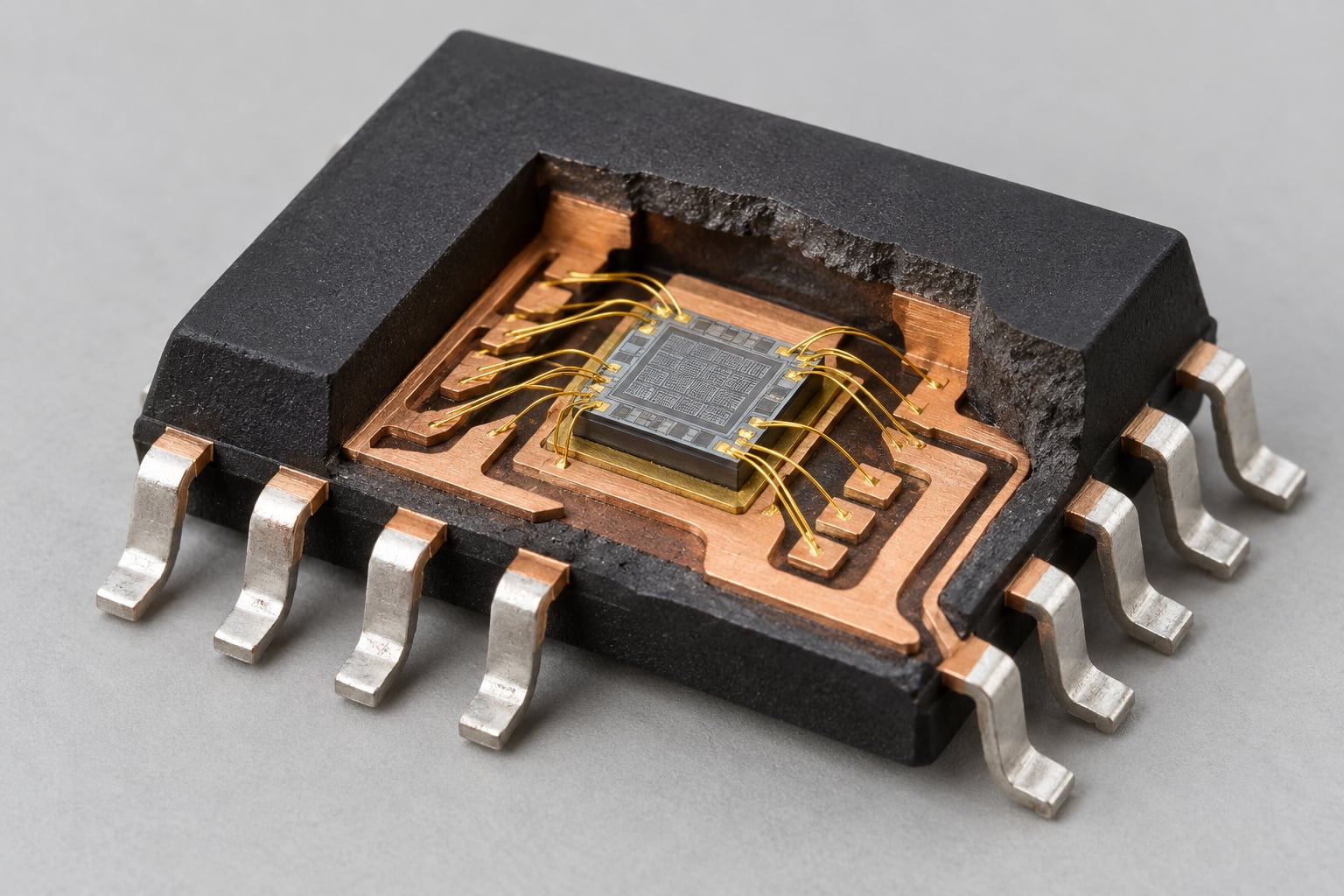
A leadframe (lead frame) is the metal frame that holds a semiconductor die during package assembly and carries its electrical connections out to the printed circuit board. Stamped or etched from copper or a copper alloy strip, it acts as the die’s carrier, its interconnect, and its main path for heat to leave the part.
That is the whole idea in two sentences. Everything else in this guide is detail layered on top of it: which features do what, how the frame is manufactured, which package families use one, and where the approach runs out of room.
Table of Contents
- What a Leadframe Is in Chip Packaging
- What Does a Leadframe Do?
- How Is a Leadframe Made?
- What Parts Make Up a Leadframe?
- What Materials Are Used for Leadframes?
- How Does a Leadframe Work in Wire-Bond Packages?
- How Does a Leadframe Work in Flip-Chip Packages?
- What Are the Main Benefits of Leadframe Packaging?
- What Are the Limitations and Design Tradeoffs?
- Leadframe vs. Other Package Interconnect Technologies
- How to Choose the Right Leadframe for a Package
- Frequently Asked Questions
- Is the leadframe the same thing as the package?
- Why is a die attached to a leadframe?
- Are bonding wires part of the leadframe?
- How does a leadframe help dissipate heat?
- Can a chip package work without a leadframe?
- Key Takeaways
What a Leadframe Is in Chip Packaging
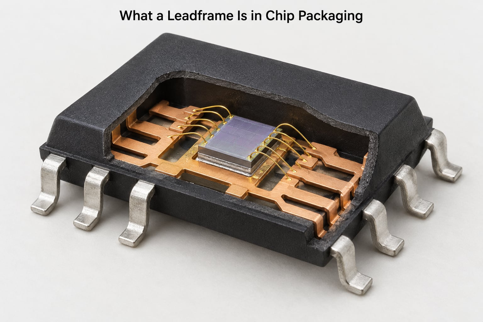
Two words, one object, and the spelling trips people up more than the physics does. “Lead frame” is the older, technically precise form used in standards and process documentation. “Leadframe” is the commercial form you see in supplier catalogs, OSAT capability lists, and equipment marketing.
Physically, a leadframe begins as a continuous strip of metal with repeating units joined by tie bars. Each unit becomes one package: a central die attach pad, a ring of leads reaching out to the edges, and a set of inner bonding fingers. After assembly the strip is cut apart, and each unit stands on its own as a finished IC.
In the classic wire-bond architecture the die sits face up in a cavity at the center of the frame, and fine gold or copper wires tie its bond pads to fingers on the frame. In flip-chip architectures the die is turned over and solder bumps or other interconnects press directly onto pads in the frame, skipping the wires entirely.
That last point matters more than it first appears. Flip-chip describes the interconnect, not the package. Many high-density devices use bumps on an organic substrate or a silicon interposer and have no leadframe at all, so it is worth separating the interconnect question from the carrier question early.
If you stripped away the molding compound and the die, what is left is essentially a stamped metal carrier with a lot of small features. Every package family below is a variation on that carrier.
What Does a Leadframe Do?
A leadframe carries out five jobs that are easy to blur together but have very different failure modes when they go wrong. Separating the structural functions from the electrical ones is usually the fastest way to understand why a given package design was chosen.
| Function | Type | What it does |
|---|---|---|
| Die support | Structural | Provides the central pad the die is attached to, keeping the die flat and in position through bonding and molding |
| Mechanical protection | Structural | Absorbs handling loads and resists warpage so the die and its bonds are not stressed during assembly or board attachment |
| Assembly handling | Structural | Gives the process equipment something rigid and uniform to grip, index, and singulate at high speed |
| Electrical routing | Electrical | Carries current from the die bond pads out to the external leads, keeping the path short and resistive losses low |
| Thermal path | Electrical | Moves heat from the die through the die attach pad and leads into the board or a heat spreader |
The die attach pad is where the structural and thermal roles overlap most. In a QFN or LFCSP that pad is deliberately left exposed on the underside of the package, so heat flows straight into the PCB land rather than through the mold compound.
The electrical job is simpler than it sounds, because the frame is metal. Copper conducts electricity roughly six times better than the organic laminate used in most substrates, so a thin frame member carries a signal with far less loss than a comparable substrate trace. The path from the top of the die to the solder pad is also short and direct, with no buried via stack sitting in between.
One more role deserves a mention: plating. The lead surfaces a bonder touches, and the leads a paste stencil touches, are almost never bare copper. A plated finish is what makes the bond reliable and the solder joint wettable.
How Is a Leadframe Made?
Every leadframe starts as a coil of metal strip. The supplier forms that strip into repeating package units, and an assembly house fills each unit with a die, wires, and plastic. The practical sequence looks like this, though the exact order varies by package and supplier.
- Form the blank. A progressive die stamps the outline of each unit from copper or alloy strip, or a wet chemical etch removes unwanted material. Stamping suits high volumes and simple outlines; etching suits complex or fine-pitch geometry.
- Plate. Electrolytic plating adds nickel as a diffusion barrier, then gold or tin on the surfaces that need conductivity, solderability, or corrosion resistance. Bonding surfaces often get a thin gold flash instead of full gold.
- Clean and inspect. Residual oils and plating chemicals are removed before bonding, because a contaminated bond pad is a delamination waiting to happen.
- Attach the die. The die is placed in the cavity and fixed with an adhesive, a conductive epoxy, or a solder or silver die-attach film, depending on the thermal budget.
- Make the interconnect. Bonding wires or clip bonds tie the die pads to the frame fingers, or the die is flipped and reflowed onto the frame pads.
- Transfer mold. The whole strip is embedded in mold compound in a single pass, with tie bars holding the leads in place during the press.
- Singulate and form. The strip is cut into individual parts by saw or punch, and the leads are cut, bent, and plated for board attachment.
- Mark and test. Parts are laser marked and tested. Many devices are tested in strip form before singulation, which is faster and cheaper than probing finished packages.
Two details make or break a frame before it ever receives a die. The first is the etch step depth, the recess that drops the lead plane below the top of the die pad so bonding wires have clearance and do not get pinched by the mold. The second is the tie bar pattern, the sacrificial connections that keep every lead in position through molding and get cut away at trim.
What Parts Make Up a Leadframe?
Names shift between suppliers and package types, but the vocabulary is fairly consistent. These are the features you will meet most often.
- Die attach pad. The central island the die is mounted on. It sets the maximum die size the package can accept and, when exposed, carries heat directly into the board.
- Support rails. The stiff members running down the length of the strip that give the frame its mechanical strength and hold the unit geometry during handling.
- Lead fingers. The outer fingers that become the package leads or lands. In a gull-wing package they bend outward and down; in a J-lead package they curl under the body.
- Bonding fingers. The short inner fingers where the bonder welds each wire or clip. They sit close together, and bond sequences are often ordered to limit tool wear.
- Tie bars. Frame material connecting one unit to the next and anchoring the leads during molding. They are cut out at trim, so their footprint is a deliberate trade against more lead area.
- Package cavity. The recess the die sits in. Its depth sets the step geometry and controls how far the die sits below the lead plane.
- Clip features. Where clip bonding replaces wire, an opposing finger pair or an L-shaped pocket is formed to hold the clip in position during the bond.
- Thermal or grounding paths. Deliberately thickened or plated features that move heat away from a hot spot or tie a lead back to the die pad for a return.
Leadless packages such as QFN and DFN change the picture slightly. There are no protruding leads to form, so the outer fingers are finished as flat lands on the bottom of the package. That is why these parts get called no-lead or leadless rather than leadframe parts, even though the frame itself is still there underneath doing the same job.
What Materials Are Used for Leadframes?
Copper and copper alloys dominate because they combine conductivity, formability, and cost in a way nothing else matches. Selection is always a compromise between properties that pull against each other: conductivity and thermal performance on one side, mechanical strength and spring resistance on the other, plus the ability to be plated, etched, and pressed without cracking.
- Copper. Highest conductivity of the group and easy to etch, but soft. Used where the frame is not heavily formed.
- C194 and C151. Copper alloys with tin or chromium added. They trade a little conductivity for real strength and better spring behaviour in formed leads.
- HCL-12S and KLF-125. High-conductivity copper alloys for parts that need both current handling and formability, common in power and automotive designs.
- TAMAC. A copper alloy family used in similar high-strength, high-conductivity applications.
- Nickel alloys and stainless steel. Used less often, where higher temperature capability or a specific corrosion profile matters more than conductivity.
On top of the base metal sits the plating system, and plating is often what actually determines bond quality. A nickel layer under the finish acts as a diffusion barrier, stopping copper from migrating into the gold or tin during thermal cycling. Tin plating is common where solderability drives the design; gold, or a thin gold flash over nickel, is common where the bonder needs a clean weldable surface.
Under-copper stress is where DAP delamination comes from in QFN parts. Copper’s coefficient of thermal expansion is roughly three times that of silicon, so a large exposed die pad on copper is a built-in stress field. Add moisture exposure at MSL 1 and the interface between pad and mold compound becomes the weak link that thermal cycling eventually finds.
How Does a Leadframe Work in Wire-Bond Packages?
In a wire-bond package the die is mounted face up on the die attach pad, active side pointing away from the pad. A bonder tool pulls a thin gold or copper wire through a hole in a capillary, presses it against a die bond pad, and welds it with a controlled burst of current or friction. The wire is then carried out to the matching bonding finger and welded there as well.
Each die pad has its own wire and its own finger, so the connection is point to point with no shared conductor. That is why wire-bonded devices tolerate years of thermal cycling without much wire fatigue: the wire can flex slightly with the package instead of being rigidly anchored at both ends.
A 32-lead TQFP makes this concrete. The die sits at the center of the frame, 32 gold wires about 25 micrometres in diameter fan out to 32 fingers, the frame is embedded in mold compound, and the fingers are cut, bent into gull-wing form, and plated with solderable tin. Trimming the outer leads away from the die pad is what makes the pitch possible at all, since the pad no longer has to be as wide as the pin spacing.
SOIC and SOT parts use the same principle with fewer pins and coarser pitch. PLCC uses a ceramic body with J-leads that insert into a socket. Different bodies, same frame logic.
How Does a Leadframe Work in Flip-Chip Packages?
In a flip-chip arrangement the die is turned over so its active face points down, and solder bumps or other conductive interconnects press it directly onto matching pads in the frame. There are no bonding wires, so the interconnect path is shorter and electrical inductance drops.
The frame still does the mechanical and thermal work. It holds the die flat through reflow, keeps the outer lands in the right coplanar relationship for the board, and provides a metal path from the die underside out to the package edge.
Again, the caveat matters. When people describe a leadframe package as flip-chip, they usually mean a frame design where the bumped die is reflowed onto the frame and the outer fingers are finished as lands. That is how many QFN and LFCSP variants are built. Where the bumps land on an organic substrate or a silicon interposer instead, there is no frame in the picture.
What Are the Main Benefits of Leadframe Packaging?
Leadframe packaging survived because it solves several problems at once that are harder to solve elsewhere. The advantages are practical rather than exotic.
- A short, direct signal path. Copper members from die pad to lead mean low resistance and low inductance, with no via stack adding delay.
- Low cost per connection. For parts with tens to a few hundred pins, a frame is a cheap way to get every pin out of the package.
- Mechanical strength. The frame gives the assembly something rigid to handle through every downstream step, from plating through final test.
- Automation fit. Bonder and molding equipment was built around this architecture, so the tooling, the handling, and the process are all mature.
- Efficient pin routing. Leads can be cut inward from different directions, so a peripheral arrangement around a small die works well.
- Good fit for small and medium I/O. Analog, mixed-signal, microcontroller, and driver parts land squarely in this range.
- Built-in thermal spread. The die attach pad spreads heat laterally before it exits through the leads or an exposed pad.
None of this makes a leadframe the cheapest option in every situation. It makes it the cheapest option for a large, well-understood band of devices, which is a bigger deal than it sounds.
What Are the Limitations and Design Tradeoffs?
The same features that make leadframes practical set their ceilings. Knowing where those ceilings sit saves a lot of wasted design work.
- I/O count and pitch. Peripheral leads need board area proportional to pin count. A device with hundreds of fine-pitch balls wants an area array, and there is no way around the geometry of leads on the edge.
- Package size and warpage. Larger molded bodies with thin leads are harder to keep flat, and coplanarity on a big QFP is one of the more common assembly problems.
- Thermal performance. Heat leaves through thin leads or a single exposed pad. A copper pad spreads heat sideways but has no path into the die except the attach material.
- CTE mismatch. Copper and silicon expand at very different rates. The stress this creates at the die attach interface is the root of delamination risk in copper-frame QFN parts, and it worsens with pad area.
- Moisture sensitivity. Exposed copper pads make these packages sensitive to moisture, so floor-life limits after baking matter more here than in a fully overmolded design.
- Parasitics and inductance. Long leads add inductance that shows up on fast edges. Manageable for control and analog parts, a real constraint for high-speed digital or RF designs.
- Wire bond scaling. Every wire occupies physical area over the die and costs a bond cycle. Thousands of bonds are a throughput problem that bump or hybrid bonding avoids.
- Handling and tooling. Every new outline, pitch, and pad arrangement is a new set of stamping dies, bonding programs, and molding tools.
This is why designers move to flip-chip, organic substrate, molded interconnect, or advanced fan-out approaches when a design needs very high I/O density, very fine pitch, very low inductance, or heavy heat removal. Those approaches cost more per unit and add process complexity, and they win because the leadframe’s geometry has stopped scaling with them.
Leadframe vs. Other Package Interconnect Technologies
There is no universal winner here. The right question is which technology fits the I/O count, thermal budget, and cost target of a specific part. The table below compares the options an engineer actually chooses between.
| Technology | Connection method | I/O density and pitch | Thermal behavior | Typical fit |
|---|---|---|---|---|
| Leadframe, wire bond | Die pad to frame finger via bonded wire, then formed lead to pad | Low to moderate; edge leads, 0.4 mm to 1.27 mm pitch | Path through die pad and thin leads; exposed pad helps on QFN | Analog, mixed-signal, MCU, drivers, automotive |
| Leadframe, flip chip | Bumped die reflowed onto frame lands | Moderate; shorter path allows tighter pitch | Good metal path from die underside to lands | Fine-pitch QFN, LFCSP, power and RF parts |
| Organic substrate (BGA, LGA) | Die on a laminate with vias and solder balls or lands | High; area array, down to sub-0.4 mm | Conductive through-via array; solder ball standoff limits top-side heat | Processors, connectivity, mobile and compute |
| Leadless (QFN, DFN) on leadframe | Wire or bump to frame lands finished flush to the bottom | Higher than gulled leads because the body perimeter is the land pattern | Exposed die attach pad directly over a board land | Power management, RF, compact modules |
| Molded interconnect device | Conductive traces molded into the plastic body | Moderate to high; traces on all sides, not just the bottom | Traces run to the outer surface and can be pulled into a heat spreader | Cost-sensitive parts needing side contacts |
| Fan-out wafer level | RDL redistributed die in a molded wafer-level package | High; no perimeter limit because routing is planar | Very short path to an exposed die side, excellent for thin devices | Mobile, connectivity, thin and small form factors |
| Silicon interposer | Bumped die on a silicon bridge with dense microbumps | Very high; sub-10 micron microbumps | Short vertical path, excellent for high-power logic | Heterogeneous integration, chiplet assembly |
The pattern is straightforward. As pin count rises and pitch falls, the metal has to be routed in more than one layer, and a single-plane peripheral-lead architecture runs out of room. That is the moment the industry moves to substrates, and later to fan-out and interposers.
In 2026 the interesting work sits at the boundary. Leadframes still dominate analog, power, automotive, and microcontrollers. At the same time, fan-out and redistribution layer processes keep pushing what a small leadframe package can carry, which is why several assembly houses now market leadframe-free lines right alongside their frame tooling.
How to Choose the Right Leadframe for a Package
Work through these in order rather than starting with a package name. The package name is the output, not the input.
- Fix the package outline. Body size, height, lead span, and seating geometry come from the package outline drawing and the land pattern. Everything else has to fit inside them.
- Check die size against the die attach pad. The pad has to be large enough for the die plus bond-landing clearance on all sides, and no larger than the cavity and mold allow. In QFN parts pad size is often a thermal decision as much as a mechanical one.
- Count I/O and set pitch. If that pin count and pitch exist as a gull-wing or J-lead outline, a leadframe package is available. If they do not, you are in substrate or fan-out territory.
- Pick the interconnect. Wire bond suits most analog and mixed-signal dies. Clip bond suits high-current devices. Flip-chip suits fine-pitch, high-speed, or low-inductance requirements.
- Select the attach method. Non-conductive die attach film for low-stress parts, conductive epoxy where a thermal or electrical path is needed, solder or silver sinter where power density is high.
- Choose base material and plating. Match the alloy to forming and spring requirements, then pick the plating system for the finish the board actually sees: tin for solderable leads, gold flash for bond surfaces, nickel barrier in both cases.
- Set thermal targets. If the part dissipates real power, decide early whether the die pad is exposed, how large it is, and what the board-side heat spreader will look like. Pad area changes with it.
- Plan warpage control. Larger bodies and thinner leads need a mold compound and fill strategy chosen for flatness, not just for cost.
- Match reliability standards. Temperature cycling, power cycling, humidity, and level MSL requirements drive plating thickness, attach materials, and pad geometry.
- Confirm tooling and capability. Check that the assembly house already runs that outline, pitch, and attach method. A new frame means new stamping tools, new bonding programs, and a qualification cycle on top of the assembly schedule.
- Validate manufacturability early. Bond pad design, tie bar layout, and etch step depth need review with the frame supplier before tape-out, not after.
Frequently Asked Questions
Is the leadframe the same thing as the package?
No. The leadframe is the metal structure inside the package, and the package is the finished assembly around it. A package includes the leadframe, the die, the bond wires or bumps, the mold compound, and whatever marking or coating is applied. Once assembly is finished the frame is partly external, because its leads form the terminals, but most of it stays hidden inside the molding. Engineers use the two terms interchangeably in conversation, which is where a lot of confusion comes from.
Why is a die attached to a leadframe?
A die is bare silicon and cannot be handled or connected on its own. Attaching it to a leadframe gives it a flat, stable surface, a defined position inside the mold, and a set of metal fingers that can be bonded or reflowed to. The attach step also sets the thermal path, which is why the adhesive, epoxy, or sintered silver choice depends on how much heat the die produces. Position, flatness, and heat spreading are the three reasons the die attach pad exists at all.
Are bonding wires part of the leadframe?
No. Bond wires are separate interconnects added during assembly, not part of the metal frame. The leadframe arrives from the supplier with plating already applied and no die attached. The bonder then welds each wire between a pad on the die and a bonding finger on the frame, and the wires become part of the electrical connection while staying mechanically distinct from the frame. Where clip bonding is used instead, the clip sits in a formed feature of the frame, but it is still an added component rather than part of the strip.
How does a leadframe help dissipate heat?
Heat leaves the die through the die attach pad and the metal of the frame, which spreads it laterally before it reaches the outside of the part. In a QFN or LFCSP the pad is left exposed so heat flows directly into a board land and copper pour rather than through the mold compound. In a gull-wing package the heat spreads along the copper leads before it reaches the solder joints. Because copper expands much faster than silicon, a large exposed pad also creates stress at the interface, so pad size is always a thermal and reliability decision together.
Can a chip package work without a leadframe?
Yes. Most high-density packages have no leadframe at all. Organic substrate packages such as BGA and LGA connect a die to a laminate board through vias and solder balls. Wafer-level chip scale packages and fan-out processes use a redistribution layer on the die or in a molded wafer-level body. Silicon interposers add a dense micro-bumped layer for heterogeneous integration. These approaches exist because a single plane of peripheral leads cannot scale to hundreds of pins or to very fine pitch.
Key Takeaways
A leadframe is two things at once: the structure that carries a die through assembly, and the electrical routing system that gets its signals out to the board. Keeping those roles separate is what makes the rest of the topic make sense, because they fail in different ways.
If you are looking at a real part, start with the architecture. Is it a wire-bond or flip-chip design, and is it a leadframe package at all? Then map the die connections: which bond pad goes to which frame finger, and through which lead. After that, inspect three things on the frame itself: the die attach pad, the bonding area, and the lead structure.
Those three features tell you most of what you need to know about thermal performance, warpage risk, and reliability before anyone builds tooling. Everything else in the frame is detail that supports them.