Decoupling capacitor placement means putting each local bypass capacitor on the same layer as the IC it serves, as close to the power pin as the design allows, and connecting it with adjacent power and ground vias so the current loop between the capacitor and the chip is as small as possible. Distance and loop area decide whether the placement works. Everything else is detail.
That is the short answer, and it hides a lot of nuance. On a board with tightly coupled power and ground planes, moving a capacitor two inches may change almost nothing. On a board with widely spaced planes or no planes at all, the same move can double the effective inductance of the connection and put the rail outside its noise budget.
This guide works through the physics first, then the placement rules, the capacitor value network, the sizing math, the via and layer choices, the failure modes, and how to check your work before the board goes to fab. I have kept the numbers in SI units and cited where each rule of thumb comes from.
A single design often mixes 1.8 V cores running at gigahertz edge rates with 12 V auxiliary rails on the same laminate, so the rules below get applied to very different circuits in one turn.
Table of Contents
- Why Decoupling Capacitors Are Placed Close to Power Pins
- How Decoupling Works During a Switching Edge
- Bypass versus decoupling: two names, one job
- The Four Rules That Control Placement Effectiveness
- Bulk, Mid-Frequency, and High-Frequency Capacitors
- Decoupling Capacitor Placement for a Single Power Pin
- Decoupling capacitor placement steps for one supply pin
- Decoupling Capacitor Placement Around an IC
- How to Calculate the Required Decoupling
- How to Choose the PCB Layer and Ground Connection
- Three placement myths worth dropping
- Via Count, Via Placement, and Plane Connections
- Decoupling Placement Problems and How to Fix Them
- How PDKs and ERC Tools Check Decoupling Quality
- Frequently Asked Questions
- How far should a decoupling capacitor be from an IC power pin?
- Should every decoupling capacitor have its own ground via?
- Is it better to place all decoupling capacitors on the top layer?
- Does capacitor distance matter if the PCB traces are short and wide?
- How many decoupling capacitors does an IC need?
- Do antipads around decoupling capacitor and ground vias increase inductance?
Why Decoupling Capacitors Are Placed Close to Power Pins
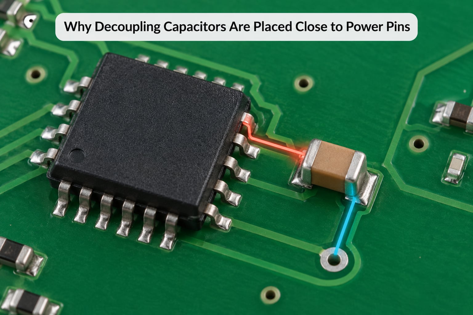
A decoupling capacitor is a small, low-inductance capacitor wired between a supply rail and ground, sitting physically next to the IC that draws current from that rail. Its job is to be the local source of transient current when the IC switches, instead of making the supply grid supply that current from somewhere across the board.
During a switching edge the IC does not draw current slowly. It steps its demand in nanoseconds, and the current has to arrive fast enough or the rail voltage collapses. A capacitor sitting at the pin can deliver that charge almost instantly, because the distance between its terminal and the pin is a few millimetres rather than a few centimetres.
The reason distance matters is inductance. Every conductor has inductance, and voltage drop across an inductor is L multiplied by di/dt. So the total path inductance between the capacitor and the pin sets how much the rail sags when the edge arrives.
The path inductance breaks into three parts:
L(path) = ESL (the capacitor’s own equivalent series inductance) + L(mount) (pad, via and solder contribution) + L(trace or plane) (the routing between capacitor and pin)
Howard Bogatin’s widely used rule of thumb puts plane spreading inductance at roughly 32 pH per square per mil of plane spacing, and closely coupled plane pairs often land near 100 pH per square. A narrow trace, by contrast, runs on the order of 5 to 7 nH per inch. That is the whole story in two numbers: a trace is about fifty to a hundred times more inductive per unit length than a plane pair.
Which is why the routing part of the equation is where designers spend their effort. You cannot change the capacitor’s own ESL, but you can absolutely change how long and how wide the connection is.
How Decoupling Works During a Switching Edge
Watch a switching edge chronologically and the role of each element in the power distribution network shows up one after the other.
First, at the instant of the edge, the local capacitor takes the transient. If the capacitor is close and its connection inductance is low, it supplies most of the step current and the rail barely moves.
Second, as the edge settles, the supply network behind it has to recharge the local capacitor and cover the average DC load. This is where plane capacitance and the DC/DC converter’s loop impedance take over. The planes act as a reservoir over a much longer timescale, and the bulk capacitance supports the load between switching converter cycles.
Third, below a certain frequency the capacitor is dominated by its ESR, and above its self-resonant frequency it behaves like an inductor. The self-resonant frequency is where the capacitive and inductive reactances cancel, and above it the part no longer helps at all.
That ordering is why a single capacitor value never covers the whole range. The part that responds to a 200 ps edge is also the part that does nothing for a 100 ms load transient, and the bulk part that handles the 100 ms is irrelevant to the edge.
One more thing happens in the second stage that surprises people: if the capacitor is far from the pin, the transient has to travel down the trace, and that trace inductance plus the pin’s own inductance form a loop with the capacitor. Voltage across that loop inductance is what shows up as droop and as radiated noise.
Bypass versus decoupling: two names, one job
The two terms get used interchangeably in most datasheets, which is why the distinction seems academic until you look at what each one emphasises. A bypass capacitor is named for what it does, shunting noise from a rail to ground. A decoupling capacitor is named for what it prevents, a transient change in supply voltage inside the chip.
Physically they are the same part in the same position. The naming difference matters only in that decoupling is the stricter role, because it asks the capacitor to supply transient current rather than merely absorb it. That is where the placement rules in this guide come from.
The Four Rules That Control Placement Effectiveness
Four things decide whether a placement is good, and they are worth listing in order because they interact.
| Rule | Recommended action | What goes wrong when you ignore it |
|---|---|---|
| Minimum distance | Shortest distance the package geometry allows; same layer as the IC whenever possible | Path inductance climbs with length, so the edge arrives late and the rail droops further than the budget allows |
| Short, wide supply and return paths | Keep both the power and the ground leg of the loop short; widen where board area allows | Loop inductance scales with loop area, so a narrow return leg undoes the benefit of a close capacitor |
| Small loop area | Put the power via and ground via adjacent to each other, on opposite polarities, with no trace between the pad and its via | A large loop radiates, and the loop inductance adds directly to the droop |
| Placement near the actual current transition | Locate the capacitor where the current actually enters the package, not on a nearby rail stub | The capacitor is on the wrong side of the package inductance, so the chip’s own IR drop lands on the rail before the capacitor sees it |
Two people will give you conflicting advice here, and both are right in context. The datasheet-style advice says put the capacitor as close as possible. The board-level advice says distribute them evenly instead of crowding them. The tie-breaker is your stackup and your package, which the sections below cover.
Bulk, Mid-Frequency, and High-Frequency Capacitors
Decoupling is a network, not a single part, and each band of the network has a different job and a different placement rule.
| Role | Typical value | Dielectric | Voltage rating | Placement role | Common packages |
|---|---|---|---|---|---|
| Bulk | 10 uF to 1000 uF | Aluminium electrolytic, polymer, or tantalum | Rated well above the rail, typically 1.5x to 2x | At the voltage entry point and near the regulator output; supports the average load between converter cycles | Radial, SMD tantalum, molded polymer |
| Mid-frequency | 1 uF to 10 uF | X5R or X7R ceramic, or polymer | 2x the rail as a derating allowance | Around the IC, typically within a few millimetres to a centimetre, spreading medium-rate current over a wider area | 0805, 1206 |
| High-frequency | 10 nF to 100 nF | C0G or X7R ceramic | 2x the rail or more | Directly at the pin, on the same layer, with adjacent vias; handles the switching edge itself | 0201, 0402, 0603 |
Ceramic capacitors lose capacitance as their DC bias rises, so a part labelled 10 uF may deliver a fraction of that at rail voltage. Pick the voltage rating with that in mind, and check the bias curve rather than the case marking.
On value ordering, the community answer is consistent: put the smallest value closest to the pin and step up in value as you move away. The small part has the highest self-resonant frequency and reacts to the fast edge; the larger part behind it covers the slower current demand.
There is a second, less obvious ordering rule. Mixing widely separated values on one net creates an anti-resonance between them, where the smaller capacitor’s impedance rises past its self-resonant frequency and meets the larger one’s rising impedance, producing a peak that can be far higher than either part alone. Paralleling identical values avoids this, because there is no capacitance ratio to resonate against.
Decoupling Capacitor Placement for a Single Power Pin
For one supply pin, the arrangement is simple enough to draw from memory, and the sequence matters more than the exact millimetres.
Decoupling capacitor placement steps for one supply pin
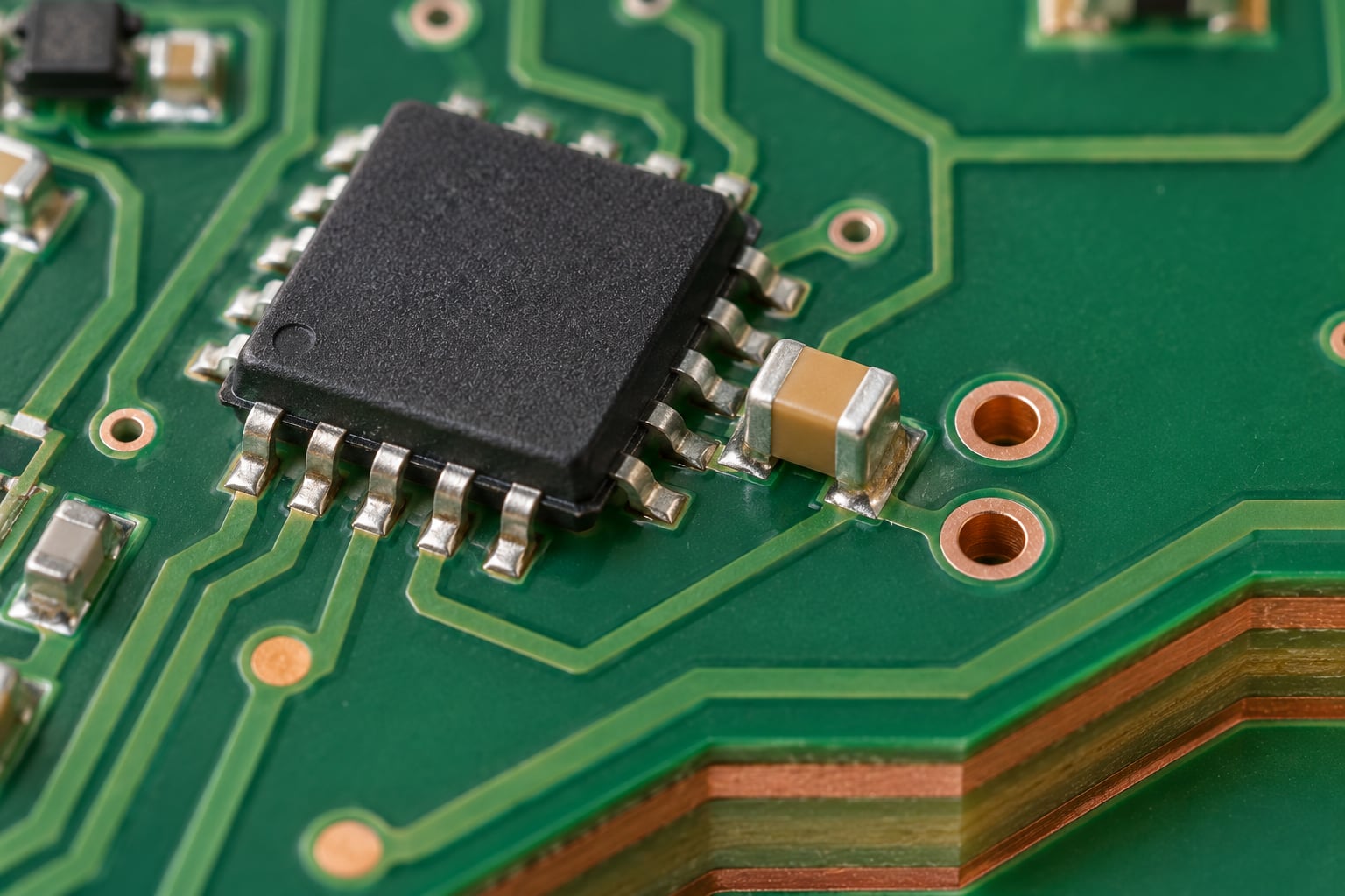
First, place the smallest capacitor directly at the pin, on the same layer as the IC. Its power pad connects to the pin or to the via that serves the pin, and its ground pad connects to an adjacent ground via with no trace in between.
Second, orient the capacitor so its ground terminal faces the nearest ground reference. This keeps the ground leg short and makes the loop area small by default rather than by effort.
Third, place the next value a few millimetres further out, in roughly the same direction along the rail, so the two capacitors form a chain along the pin rather than a cluster in one spot.
Fourth, add bulk capacitance at the point where the rail enters the board or at the converter output, not at the pin. Its job is a different timescale, so proximity to the pin buys nothing.
Daniel Beeker at NXP puts the useful distance in terms of the edge itself: the capacitor should sit within a fraction of the distance the edge propagates along the connection during the transition. That reframes the question usefully, because it means the limit moves with rise time rather than being a fixed number.
Decoupling Capacitor Placement Around an IC
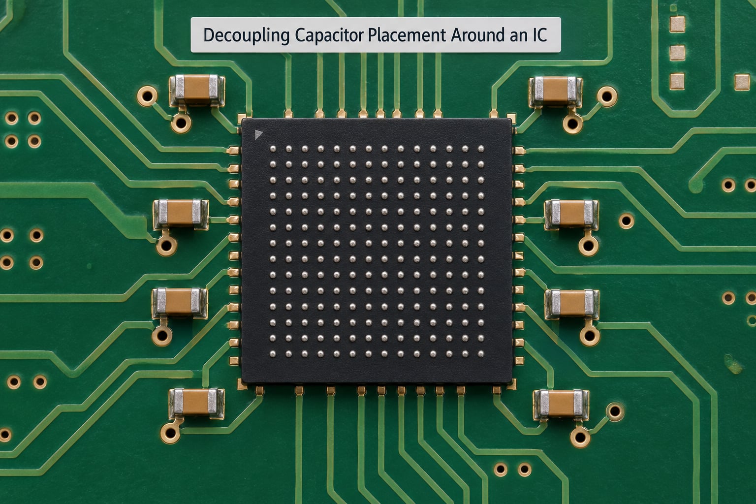
Single-pin logic scales to a package, but the constraints get tighter as pin count rises. Around a QFP or QFN there is usually room on all four sides, and the job is mostly about keeping loops short and avoiding crowding. Under a BGA there may be no room on the top layer at all, so the rules change.
For leaded packages, place a high-frequency capacitor at each supply pin or at each small group of pins, and put the ground via immediately beside it. Keep the current’s entry point and its return point physically together.
For BGA packages, the pin connection is a via into the package, so the capacitor needs to reach the plane, not the pin. The usable set of rules is short enough to state as a list:
- Connect every decoupling capacitor to the power and ground planes through adjacent vias, because there is no top-layer escape from most balls.
- Give each capacitor its own ground via rather than sharing one with a neighbour.
- Place the via pair directly beside the capacitor pad, with no trace routed between the pad and the via.
- Keep the fanout vias from the BGA aligned so the capacitor’s via can land on the nearest power or ground ball.
- Where interior power and ground balls are available, use them rather than only the outer ring, which spreads current more evenly across the package.
- For components on the far side of the package, connect to the planes that feed the nearest balls rather than reaching around the package.
- Do not route signal traces through the decoupling region, since they break up the plane and force current around them.
- Leave the assembly and rework escape routes open, so the capacitor can be replaced without removing neighbouring parts.
That last rule fights the other seven, and it wins often. Lee Ritchey of Speeding Edge described a 10 Gbps line card with a 2,000-pin BGA where capacitors crammed under the package were nearly irrelevant because the tightly coupled planes were already doing the work, and the cramming made assembly and rework miserable. Distributing rather than crowding is the better trade when the planes are good.
Avoid mixing dedicated analog rails with digital ones. A separate decoupling network per rail, each with its own return, keeps switching return current out of the analog reference.
How to Calculate the Required Decoupling
The calculation is a first-pass estimate, not a guarantee, and it is worth doing anyway because it tells you whether the number of capacitors in the schematic is in the right order of magnitude.
Start with target impedance, the value the PDN impedance should stay below across the band you care about:
Z(target) = maximum allowable ripple / maximum instantaneous current
Steve Sandler at Picotest is the reference most engineers cite for this, and it pairs with a companion expression for how much capacitance a target impedance implies:
C = L / (R squared)
where L is the effective inductance of the connection and R is the target impedance.
The frequency band the network has to cover comes from the rise time of the fastest edge in the design. The common conversion is bandwidth = 0.35 / rise time, so a 1 ns edge asks the network to stay flat to roughly 350 MHz.
Take a worked example. A processor core draws a 20 A transient for 500 ns on a 1.8 V rail, and you allow 50 mV of droop. Target impedance is 50 mV divided by 20 A, which is 2.5 mOhm. If the connection inductance works out at 1 nH, the capacitance implied by the companion formula is a few nanofarads spread across a band whose top edge sets the count.
Now compare two ways of moving current five inches from a bulk capacitor to that pin, which is the calculation that changes minds.
| Connection method | Inductance per unit length | Inductance over 5 inches | Relative to the trace case |
|---|---|---|---|
| Narrow routed trace | About 5 nH per inch | About 25 nH | Baseline |
| Wider routed trace | Roughly 3 to 5 nH per inch | About 15 to 25 nH | Modest improvement, area expensive |
| Closely coupled plane pair at about 100 pH per square | About 100 pH per square, roughly 2 to 3 squares over 5 inches | About 0.25 nH | Around one hundred times lower |
The figures are the ones Hubing’s group and Altium both work from, and dielectric spacing moves the plane number further still. Same physical distance, two orders of magnitude apart.
Where the estimate breaks down: package inductance, tolerance, ESR, the transient’s actual duration, and whether the capacitor’s self-resonant frequency sits inside your band. Treat the number as an order of magnitude and verify with simulation.
How to Choose the PCB Layer and Ground Connection
The layer a decoupling capacitor sits on changes its behaviour, and so does the plane spacing underneath it.
On the component side, the capacitor has the shortest possible path to the pin and the least vertical distance to the reference plane. This is where local decoupling belongs whenever there is room.
On a signal layer immediately adjacent to the plane pair, the capacitor gains the plane capacitance of that pair but pays for it with a longer vertical path through a via. On deeper plane layers, you lose local placement entirely and end up with spreading inductance alone.
What sits underneath matters more than which layer the capacitor occupies. A closely coupled power and ground pair, roughly 10 mil or less apart, stores energy in the dielectric between the planes and spreads current quickly. Widen the spacing to 40 mil on a four-layer board and the spreading inductance rises sharply, which is why the same capacitor value behaves differently on different laminate builds.
Hubing and his coauthors at IEEE published the threshold that most designers now cite: below about 10 mil of plane spacing, decoupling becomes remarkably insensitive to where the capacitor sits, because the planes are carrying the transient for you. Above that, placement starts to matter again.
The three plane configurations behave differently enough to be worth stating side by side, because the rule you should follow depends entirely on which one you have.
| Plane configuration | Spreading inductance | How much placement matters | Recommended approach |
|---|---|---|---|
| No power or ground planes (routed power only) | Trace inductance only, roughly 5 to 7 nH per inch | Everything. Distance is the dominant term | Shortest possible path per pin, wide conductors, adjacent opposite-polarity vias, extra capacitance since each part carries more |
| Closely coupled plane pair, about 10 mil or less | On the order of 100 pH per square, with useful plane capacitance | Little, within roughly a centimetre of the pin | Distribute capacitance evenly rather than crowding, keep vias adjacent, keep the pair coupled through the build |
| Widely spaced plane pair, 40 mil or more on a four-layer board | Rises steeply with spacing; the AMD-published figures are about 130 pH per square at 4 mil, 65 at 2 mil and 32 at 1 mil | Substantial. The planes no longer cover for you | Revert to close placement, widen the plane spacing budget if mechanical allows, or move to a build with more layers |
This result gets over-generalised more than any other in the field. It holds for the plane configuration studied, and it does not rescue a board with no planes, a BGA whose current cannot reach a plane, or a rail with a genuinely fast edge.
Three placement myths worth dropping
Closer is always better. It is better, up to the point where you start trading away plane access, or the layout stops being manufacturable. On a well-coupled stackup the difference between 2 mm and 15 mm is usually noise in the impedance curve, and the crowded version costs you rework access for nothing.
More capacitors fix a bad layout. They do not, and this one wastes board area quietly. Parts sitting further out raise capacitance on a path whose inductance still dominates the impedance at that frequency, so the rail behaves exactly as before. Move the parts inward or shorten the loop first, then count again.
Ultra-low-ESL parts are always the answer. A specialty low-inductance package still has mounting inductance, and mounting inductance is often the larger term once the part reaches a via and a plane. Steve Sandler and others have argued the point for years: a 0402 or 0603 part with a well-placed adjacent via often beats an expensive low-ESL part mounted through the same mediocre connection. Judge the whole path, not the datasheet label.
Via Count, Via Placement, and Plane Connections
The via arrangement is the part of decoupling placement that most often gets drawn wrong, because it looks like a minor routing decision.
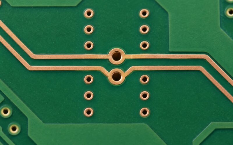
A single ground via next to the capacitor pad is acceptable when the loop is small and the current share is modest. Two vias help when you are sharing the connection, when the via is long, or when the pad is far from any plane. A pair of vias of opposite polarity, one for power and one for ground, placed side by side, is the standard answer.
Three specific habits prevent most of the avoidable loss. Do not route a trace between the capacitor pad and its via. Do not share a ground via between two adjacent capacitors, because the shared via becomes the choke in the loop. Do not let the ground via land on a split or a different net, even if the schematic says it is ground.
Via-in-pad removes the via from the loop entirely and is genuinely useful under a BGA where there is no room beside the part. It carries real cost: it needs a filled and capped via for solder control, it complicates the design for any assembly house that reflows by hand, and it slows down respinning the design. On most boards a well-placed via beside a 0402 or 0603 pad lands within a few hundred picohenries of the same goal.
Antipads matter too. A cleared antipad around the via and around the capacitor’s own pads removes copper, and that removed copper is where the current has to detour. Large antipads under a plane couple directly to adjacent planes and raise the effective inductance of the connection. Tenting or bonding the via, where the fab allows it, recovers some of that.
Decoupling Placement Problems and How to Fix Them
Most placement faults show up as a symptom you can measure. Matching the symptom to the cause is faster than staring at the layout.
| Symptom | Likely cause | Fix |
|---|---|---|
| Device resets or erratic behaviour when a relay or motor switches | Transient from another rail coupling onto the sensitive supply through a shared loop or shared via | Separate the decoupling networks per rail and give each its own ground via |
| Rail rings or oscillates only after adding capacitors | Anti-resonance between differing values, or a feedback loop with the regulator | Parallel identical values instead of mixed ratios, and check the converter’s compensation |
| Droop or brownout on a load step, worse when warm | Path inductance too high, or bulk capacitance placed away from the entry point | Shorten the path, move bulk capacitance to the entry point, add local capacitance at the pin |
| Fails radiated emissions, passes conducted | Large loop area, often from a shared ground via or an antipad detour | Adjacent opposite-polarity vias, smaller antipads, via tenting or bonding |
| Works on the bench, fails in the enclosure | Bulk capacitance too close to the entry point only, with nothing local under load | Distribute capacitance across the board instead of concentrating it at the connector |
| Timing errors that come and go with temperature | Ceramic DC bias derating reducing real capacitance below the calculated value | Re-check against the bias curve, raise the voltage rating, or add parallel parts |
One symptom deserves its own note, because it is the most common complaint on engineering forums. Adding capacitors and seeing no improvement almost always means the loop is the problem, not the count. Extra parts sitting further out add capacitance to a path whose inductance still dominates the impedance at that frequency.
And a caution about stacking rules: putting capacitors directly beneath a BGA is often quoted as good practice and is frequently an assembly and rework mistake. Cramming parts under a package you may need to replace is a cost that shows up after the first return, not before.
How PDKs and ERC Tools Check Decoupling Quality
The foundry and vendor tools can tell you whether you broke a rule. They cannot tell you whether the board works.
Foundry PDK design rules cover the things a rule checker can measure: via counts and via diameters on power nets, antipad geometry, minimum spacing between planes, current density limits, and decoupling requirements stated for specific packages. Application notes from the IC vendor add guidance on capacitance value, count, and permitted distance from the pin, and ERC tools flag violations of those locally.
Those are guardrails, not verification. Passing every decoupling rule is compatible with a board that fails emission testing, which is exactly why nobody should stop at a green rule check.
Real verification is frequency-domain. Build a PDN impedance model of the planes, the vias, and the capacitors as an equivalent circuit, then sweep it and look for two things: whether the impedance stays below your target across the band the edge requires, and whether any resonance peak sits inside that band. A peak inside the band is the anti-resonance problem, and it is visible in a plot long before it is visible on a bench.
Do that model twice, once on a rough placement and once on the final routed layout. The difference between the two tells you how much your placement decisions actually bought you, which is the number most useful in a design review.
One habit from Electronics StackExchange threads is worth keeping: compare a board that works against one that does not, and read the two impedance curves side by side. That comparison settles arguments about placement rules faster than any amount of theory, because it uses your own stackup and your own capacitor set.
Frequently Asked Questions
How far should a decoupling capacitor be from an IC power pin?
On a board with a closely coupled power and ground plane pair, roughly 10 mil or less apart, distance matters little because the planes carry the transient for you. On widely spaced planes or boards without planes, put the high-frequency capacitor on the same layer as the IC, within a few millimetres of the pin, and treat any increase in distance as added path inductance of roughly 5 to 7 nH per inch.
Should every decoupling capacitor have its own ground via?
Yes, as a default. A shared ground via becomes the choke in the current loop and adds inductance that no amount of extra capacitance recovers. Place each capacitor’s ground via directly beside its pad with no trace in between, and use a power and ground via pair of opposite polarity next to each other on the component side.
Is it better to place all decoupling capacitors on the top layer?
Local high-frequency decoupling belongs on the component side, next to the pin, because that gives the shortest path and smallest loop area. Bulk capacitance belongs at the voltage entry point or the converter output instead, where it supports the load between converter cycles. Putting everything in one place wastes the low-frequency benefit of the bulk parts.
Does capacitor distance matter if the PCB traces are short and wide?
Less than it would on a narrow trace, but not zero. Loop inductance scales with loop area, so widening both legs helps roughly as much as shortening them. The saving is partial: inductance falls with loop area rather than vanishing, and you still pay the mounting and pad inductance that no amount of trace width removes.
How many decoupling capacitors does an IC need?
Size the network instead of counting parts. Set a target impedance from the allowable ripple and the maximum instantaneous current, derive the frequency band from the fastest edge using bandwidth = 0.35 divided by rise time, then add values so the network stays under that target across the band. Typical starting points are one 10 to 100 nF part per supply pin plus one 1 to 10 uF part per device, then verify by simulation.
Do antipads around decoupling capacitor and ground vias increase inductance?
They do, because cleared copper forces current to detour around the opening. A large antipad under a plane also couples to the adjacent layer and weakens plane capacitance. Tenting or bonding the via where your fabricator allows it recovers part of that loss, and it is one of the cheaper fixes available on an existing layout.
Start with your stackup, not with the rule list. If the power and ground planes are closely coupled, you have slack on distance and can distribute capacitance evenly while keeping parts accessible. If they are widely spaced, or you have no planes, every millimetre of trace counts, so push the smallest values to the pins and give each capacitor its own adjacent ground via.
Decoupling capacitor placement comes down to that one decision plus a PDN impedance check on your own layers, which will tell you whether any resonance peak lands inside the band your fastest edge occupies. Confirm it rather than assuming.